


下载
2010 Microchip Technology Inc. DS01327A-page 1
AN1327
INTRODUCTION
This application note describes how to avoid MOSFET
driver overstress. MOSFET drivers are used in many
applications to drive the high input capacitance of a
power MOSFET device. MOSFET drivers are very reli-
able when used within their operating specifications.
Care must be taken, however, to control supply line
transients and power dissipation, and prevent latch-up.
AVOIDING SUPPLY LINE
TRANSIENTS
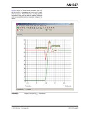
During switching transitions, parasitic inductances can
create transients on the supply line, and those can cre-
ate electrical overstress. Proper bypass capacitor
selection and PCB layout must be performed to protect
the driver from voltage transients during switching tran-
sitions. Proper PCB layout is necessary to minimize
parasitic inductance in the supply path, and the ground
path.
Microchip provides MOSFET driver models for the
following devices:
- TC1410
-TC1411
- TC1412
- TC4404/05
- TC4420/29
- TC4421/22
- TC4423/24/25
- TC4423A/24A/25A
- TC4426/27/28
- TC4426A/27A/28A
- TC4431/32
- TC4451/52
- TC4467/68/69
These driver models can be downloaded from the
Microchip web site, www.microchip.com.
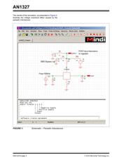
Simulating Supply Line Transients
The Mindi™ Circuit Designer and Simulator can be
used to simulate supply line transients. (Mindi software
can be downloaded from the Microchip web site.) The
following simulation includes the parasitic inductances
that are associated with package inductance, bypass
capacitor parasitic series inductance, and printed wir-
ing board inductance.
The PCB Trace Inductance diagram in Figure 1 shows
the TC4423A device (3A peak output current) in a
circuit with following items:
• L4 – parasitic inductance in series with ground pin
• L5 – parasitic inductance in series with V
DD
pin
• L1, L2 – parasitic inductance in series with the
bypass capacitor
• Capacitor C2 (1 nF) is used to represent the
MOSFET
• L3 – the inductance from the TC4423A device to
the power source
Note that the inductance between the driver output and
C2 (MOSFET) is not included in this circuit simulation,
but should be included in common practice. Addition-
ally, the driver should be located as close to the output
MOSFET as possible.
GETTING STARTED
Before simulation can begin, a symbol for the MOSFET
driver must be created, and a MOSFET driver model
netlist must be assigned to that symbol. Pressing the
F11 key in Mindi opens a window where the model
netlist can be copied, and the symbol can be assigned
to that model netlist.
For example, assume that the following characteristics
are applied to the items in the simulated circuit in
Figure 1:
• L4 and L5 – SOIC package leads PCB trace =
10 nH
• L1 and L2 – series inductance of a 0805 ceramic
capacitor PCB trace = 10 nH
• L3 – PCB trace inductance from the V
DD
pin to
the power source that feeds the MOSFET driver
Note that the parasitic series resistance and input/out-
put PCB inductance have been omitted from this
simulation, but they are available for inclusion.
Author: Ray DiSilvestro
Microchip Technology Inc.
Avoiding MOSFET Driver Overstress