
下载

Application Report
SLEA025A – NOVEMBER 2003
1
Voltage Spike Measurement Technique and Specification
Claus Neesgaard, Cetin Kaya, Fred Shipley Digital Audio
ABSTRACT
As an extension to the voltage ratings given in the Absolute Maximum Ratings section of
TAS5111, TAS5112, TAS5121 and TAS5122 data sheets this application note gives a
more explicit description of the maximum limit for peak voltage vs. time on the BST and
OUT pins. Additionally, a measurement technique and test setup is described and
application design guidelines given on how to avoid exceeding the device voltage
limitation defined as envelope curves.
Contents
1
Introduction ..................................................................................................................................2
2 Background ..................................................................................................................................2
3 Absolute Maximum Voltage vs. Time..........................................................................................3
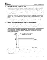
3.1 Absolute Maximum Voltage vs. Time on BST_X, Normal Operation.......................................3
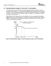
3.2 Absolute Maximum Voltage vs. Time on BST_X, Fault Situation.............................................4
4 Voltage Spike Measurement Technique......................................................................................5
4.1 Equipment (Oscilloscope and Probes)....................................................................................5
4.2 Test Setup..............................................................................................................................6
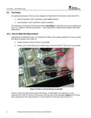
4.2.1 How to Make the Measurement...................................................................................6
4.2.2 Normal Operation - Test Setup....................................................................................7
4.2.3 Fault Situation - Test Setup.........................................................................................8
5 Recommended configuration......................................................................................................9
5.1 PCB Layout.............................................................................................................................9
5.2 Bootstrap Series Resistor .......................................................................................................9
5.3 Transient Voltage Suppressors (TVS)...................................................................................10
Figures
Figure 1 Abs Max Voltage vs. TIme, Rising Edge Transition on BST, Normal Operation ...............3
Figure 2 Abs Max Voltage vs. Time, Rising Edge Transition on BST, Fault Situation.....................4
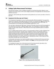
Figure 3 This is how the ground wire should look.............................................................................5
Figure 4 Probe as close to the pin as possible..................................................................................6