

下载

AFIC901N
1
RF Device Data
Freescale Semiconductor, Inc.
RF LDMOS Wideband Integrated
Power Amplifier
The AFIC901N is a 2--stage, high gain amplifier designed to provide a high
level of flexibility to the amplifier designer. The device is unmatched even at the
interstage, allowing performance to be optimized for any frequency in the 1.8 to
1000 MHz range. The high gain, ruggedness and wideband performance of this
device make it ideal for use as a pre -- driver and driver in a wide range of
industrial, medical and communications applications.
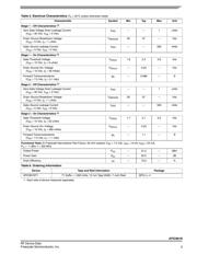
Typical Narrowband Performance
(7.5 Vdc, T
A
=25C, CW)
Frequency
(MHz)
G
ps
(dB)
D
(%)
P
out
(dBm)
520
(1)
32.2 73.0 31.2
Typical Wideband Performance (7.5 Vdc, T
A
=25C, CW)
Frequency
(MHz)
P
in
(dBm)
G
ps
(dB)
D
(%)
P
out
(dBm)
136–174
(2,5)
0 30.6 62.1 30.6
350–520
(3,5)
3 27.4 61.5 30.4
760–870
(4,5)
3 27.6 57.0 30.6
Load Mismatch/Ruggedness
Frequency
(MHz)
Signal Type VSWR
Pin
(W)
Test
Voltage
Result
175
(2)
CW > 25:1 at all
Phase Angles
3dB
Overdrive
from rated
power
9 No Device
Degradation
520
(3)
1. Measured in 520 MHz narrowband test circuit.
2. Measured in 136–174 MHz VHF broadband reference circuit.
3. Measured in 350–520 MHz UHF broadband reference circuit.
4. Measured in 760–870 MHz broadband reference c ircuit.
5. The values shown are the center band performance numbers across the indicated
frequency range.
Features
Characterized for Operation from 1.8 to 1000 MHz
Unmatched Input, Interstage and Output Allowing Wide Frequency Range
Utilization
Integrated ESD Protection
Same PCB Layout Can be Used for 136--174 MHz, 350--520 MHz and
760–870 MHz Designs.
24--pin, 4 mm QFN Plastic Package
Typical Applications
Driver for Mobile Radio Power Amplifiers
Output Stage for Low Power Handheld Radios
Driver for Communications and Industrial Systems
Document Number: AFIC901N
Rev. 0, 1/2016
Freescale Semiconductor
Technical Data
1.8–1000 MHz, 30 dBm, 7.5 V
AIRFAST RF LDMOS WIDEBAND
INTEGRATED POWER AMPLIFIER
AFIC901N
QFN 4 4
Figure 1. Pin Connections
Note: Exposed backside of the package is the
source terminal for the transistors.
RF
in
RF
out
External
Interstage Match
Figure 2. Typical Application
GND
GND
24 23
1
2
3
4
5
6
N.C.
N.C.
N.C.
N.C.
N.C.
N.C.
GND
N.C.
Drain B
GND
N.C.
Gate B
Gate A
N.C.
N.C.
Drain A
Drain B
Drain B
Gate B
Gate B
22 21 20 19
7
8
9 10 11 12
18
17
16
15
14
13
Gate A
Drain A
Stage 1
Stage 2
Stage 2Stage 1
Freescale Semiconductor, Inc., 2016. All rights reserved.
页面指南