


下载
October 2010 Doc ID 17962 Rev 1 1/32
AN3275
Application note
Improving the performance of smartcard interfaces
using the ST8024L
Introduction
The ST8024L is a smartcard interface offered as a drop-in replacement for the ST8024
device. Enhancements and changes to the ST8024L device include:
● Improved performance by reducing the noise sensitivity in the charge pump
● Incorporated 1.8 V V
CC
output
● Lower V
TH
threshold voltage
This application note provides information and suggestions for the optimal use and
performance of the ST8024L smartcard interface, including PCB layout, external component
placement, and connections (see ST8024L application hardware guidelines on page 18).
The implementation of all the blocks and procedures for card activation and deactivation
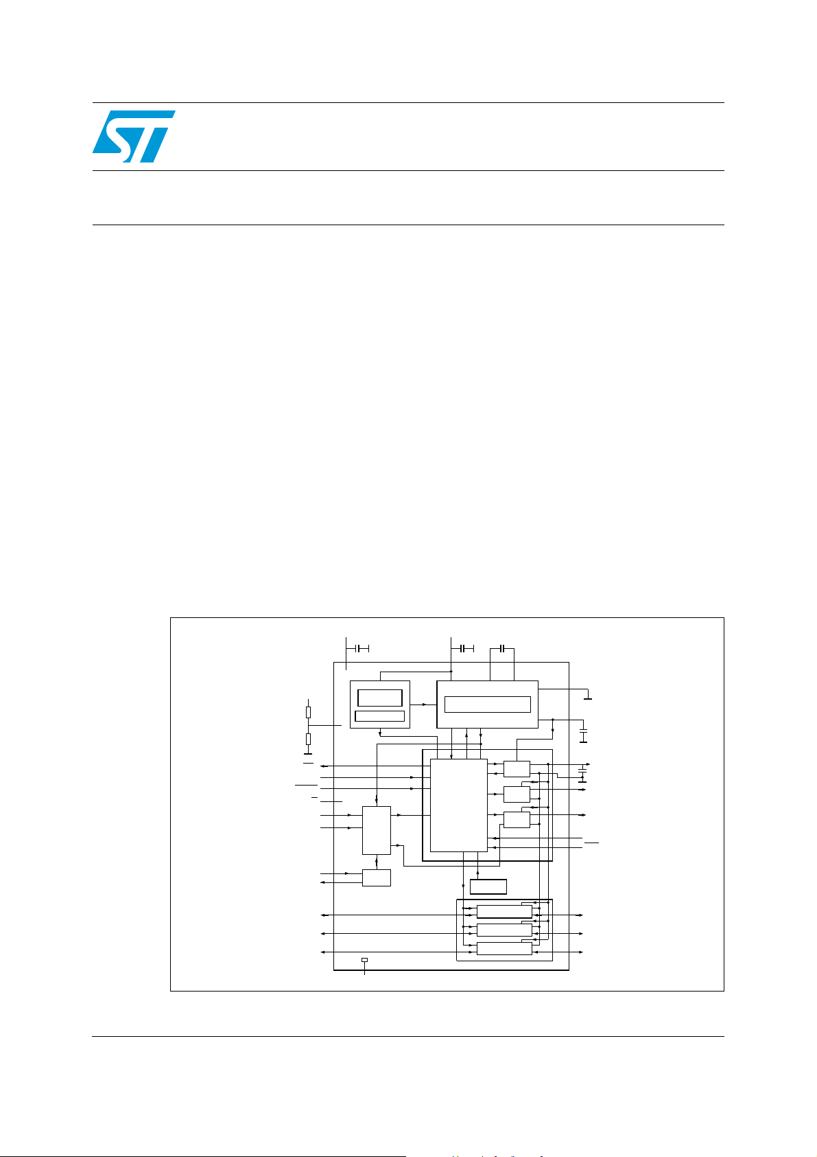
(see Figure 1) of the smartcard are also explained.
The ST8024L is a smartcard interface designed to minimize microprocessor hardware and
software complexity in all applications that require a smartcard (e.g., set-top box, electronic
payment, pay TV, and identification cards). The electrical characteristics of the ST8024L are
in accordance with New Digital Systems (NDS) and compliant with ISO7816-3, GSM11.11,
and EMV 4.0. Two devices (ST8024LCDR and ST8024LCTR) in the ST8024L family have
been certified by NDS.
Figure 1. ST8024L internal block diagram
CS18100
ST8024L
C1–
C1+
18
PORADJ/1.8V
SEQUENCER
OSCILLATOR
CLOCK
CIRCUITRY
CLK
HORSEQ
THERMAL
PROTECTION
CLOCK
BUFFER
I/O
TRANSCEIVER
I/O
TRANSCEIVER
I/O
TRANSCEIVER
RST
BUFFER
V
CC
GENERATOR
INTERNAL OSCILLATOR
2.5 MHz
STEP-UP CONVERTER
ALARM
POWER_ON
EN1
CLKUP
EN2
PV
CC
EN5
EN4
EN3
VOLTAGE SENSE
INTERNAL
REFERENCE
SUPPLY
21 6
7
5
100nF 100nF
V
DDP
100nF
V
DD
23
20
19
3
1
2
CLKDIV2
(2)
CLKDIV2
(1)
5V/3V
CMDVCC
RSTIN
OFF
V
DD
V
ref
R
2
(1)
R
1
(1)
XTAL1
XTAL2
(2)
24
25
27
28
26
22
AUX1UC
(2)
AUX2UC
(2)
I/OUC
GND
4
8
V
UP
PGND
100nF
V
CC
100nF
CGND
RST
CLK
PRES
PRES
(2)
AUX1
(2)
AUX2
(2)
I/O
17
14
16
15
10
9
13
12
11
www.st.com