


下载
1
www.pericom.com P-0.1 01/24/11
PI49FCT20802/PI49FCT20803
1:5/1:7 2.5V Clock Buffer for
Networking Applications
Description
e PI49FCT2080x is 2.5V, high-speed, low noise, non-inverting
clock buer. It is designed to target networking applications that
require low-skew, low-jitter, and high-frequency clock distribu-
tion. It provides output-to-output skew as low as 150ps, and
is an ideal clock distribution device for synchronous systems.
PI49FCT2080x is a clock buer from a single input that pro-
duces ve outputs on PI49FCT20802 and seven outputs on
PI49FCT20803. PI49FCT2080x is characterized for operation
from –40°C to 85°C.
Features
Î High Frequency >150 MHz
Î High-speed, low-noise, non-inverting clock buer
à PI49FCT20802 is a 1:5 buer
à PI49FCT20803 is a 1:7 buer
Î Low skew < 150ps
Î Low duty cycle distortion < 300ps
Î Low propagation delay < 3.5ns
Î Multiple V
DD
, GND pins for noise reduction
Î 2.5V supply voltage and 3V tolerant input
Î Packaging (Pb-free & Green):
à 16-pin TSSOP (L)
à 16-pin QSOP (Q) - PI49FCT20802 only
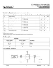
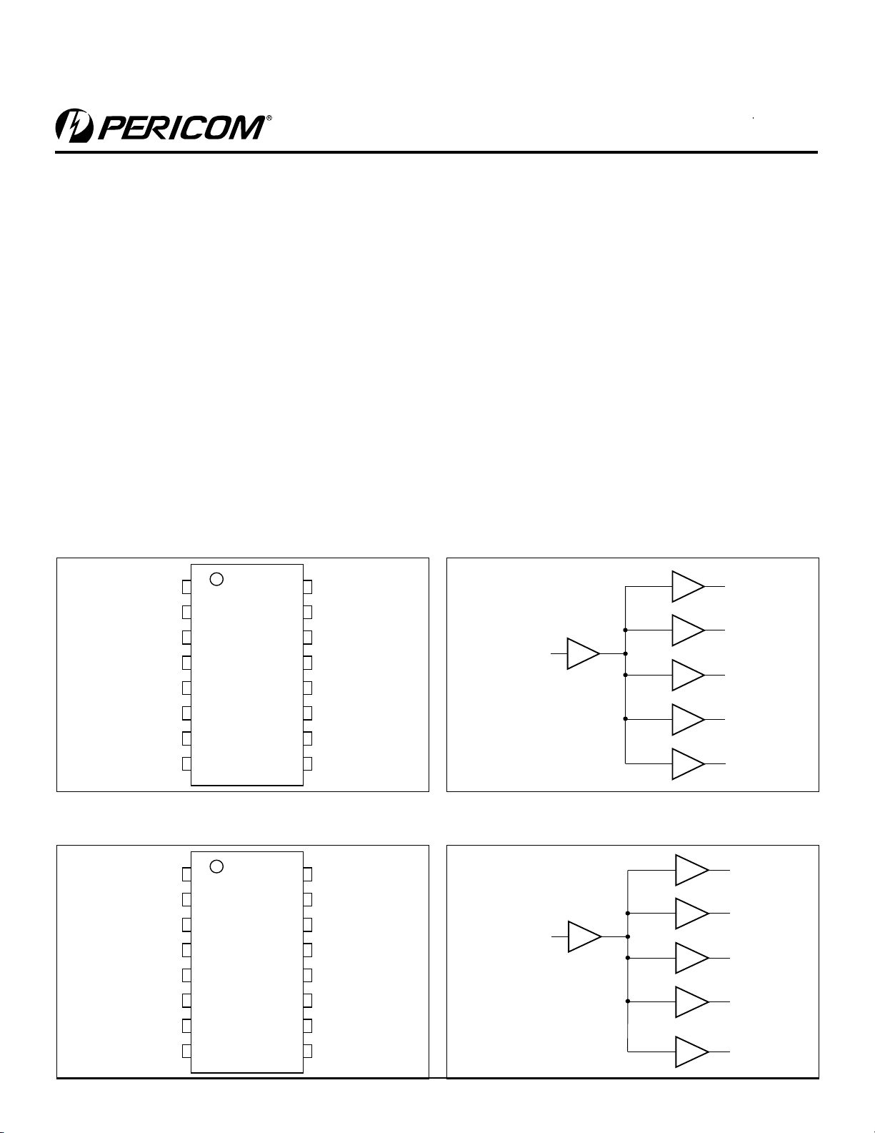
Pin Configuration (PI49FCT20802)
1
2
3
V
DD
4
CLK1
5
CLK0
6
NC
7
V
DD
8
GND
V
DD
CLK3
GND
V
DD
NC
GND
16
15
14
13
12
11
10
9
BUF_IN
GND
CLK2
CLK4
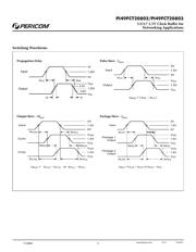
Block Diagram (PI49FCT20802)
CLK4
CLK2
CLK1
CLK0
BUF_IN
CLK3
Block Diagram (PI49FCT20803)
CLK6
CLK2
CLK1
CLK0
BUF_IN
CLK3
. . .
Pin Configuration (PI49FCT20803)
1
2
3
V
DD
4
CLK1
5
CLK0
6
CLK2
7
V
DD
8
GND
V
DD
CLK5
GND
V
DD
CLK3
GND
16
15
14
13
12
11
10
9
BUF_IN
GND
CLK4
CLK6
11-0004
页面指南