
下载

Application Report
SBOA094 - August 2003
1
Measuring Board Parasitics in High-Speed Analog Design
Rea Schmid High Speed Produc
ts
ABSTRACT
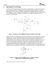
Successful circuit designs using high−speed amplifiers can depend upon understanding and
identifying parasitic printed circuit board (PCB) components. Simulating a design while
including PCB parasitics can protect against unpleasant production surprises. This
application report discusses an easy method for measuring parasitic components in a
prototype or final PC board design by using a standard oscilloscope and low frequency
waveform generator to collect valuable information for SPICE simulation.
Contents
1 High Speed Circuit Design 2. . . . . . . . . . . . . . . . . . . . . . . . . . . . . . . . . . . . . . . . . . . . . . . . . . . . . . . . . . .
2 Determining the Source of the Capacitance 3. . . . . . . . . . . . . . . . . . . . . . . . . . . . . . . . . . . . . . . . . . . .
3 Capacitive and Inductive Measurement Techniques 4. . . . . . . . . . . . . . . . . . . . . . . . . . . . . . . . . . . .
4 Measurement Notes and Aids 8. . . . . . . . . . . . . . . . . . . . . . . . . . . . . . . . . . . . . . . . . . . . . . . . . . . . . . . . .
List of Figures
Figure 1. Example Circuit for 900MHz Frequency Amplifier, Gain 2 Stage 2. . . . . . . . . . . . . . . . .
Figure 2. Example Circuit for 900MHz Frequency Amplifier, Gain 2 Stage,
with Parasitic Inverting Node Capacitance 2. . . . . . . . . . . . . . . . . . . . . . . . . . . . . . . . . . . . .
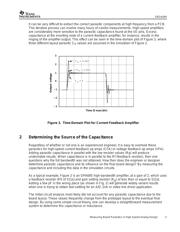
Figure 3. Time−Domain Plot for Current Feedback Amplifier 3. . . . . . . . . . . . . . . . . . . . . . . . . . . . .
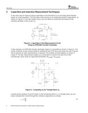
Figure 4. Capacitance Test Measurement Circuit Using an HP8116A Function Generator 4. . .
Figure 5. Computing V
2
for a Triangle Wave V
1
4. . . . . . . . . . . . . . . . . . . . . . . . . . . . . . . . . . . . . . . . .
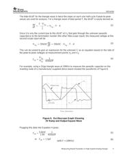
Figure 6. Oscilloscope Graph Showing 2V Ramp and Output Square Wave 5. . . . . . . . . . . . . . .
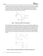
Figure 7. Measuring a Parasitic Trace Inductance 6. . . . . . . . . . . . . . . . . . . . . . . . . . . . . . . . . . . . . . .
Figure 8. Stimulus and Response Waveforms for Parasitic Inductance Test 6. . . . . . . . . . . . . . .
Figure 9. Scope Preamp for Capacitance Measurement 8. . . . . . . . . . . . . . . . . . . . . . . . . . . . . . . . . .
Figure 10. Scope Preamp for Inductance Measurement 8. . . . . . . . . . . . . . . . . . . . . . . . . . . . . . . . . . .
All trademarks are the property of their respective owners.