
下载
© Semiconductor Components Industries, LLC, 2001
October, 2016 − Rev. 6
1 Publication Order Number:
MMBT489LT1/D
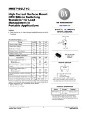
MMBT489LT1G
High Current Surface Mount
NPN Silicon Switching
Transistor for Load
Management in
Portable Applications
Features
• These Devices are Pb−Free, Halogen Free/BFR Free and are RoHS
Compliant
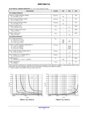
MAXIMUM RATINGS (T
A
= 25°C)
Rating
Symbol Max Unit
Collector-Emitter Voltage V
CEO
30 Vdc
Collector-Base Voltage V
CBO
50 Vdc
Emitter-Base Voltage V
EBO
5.0 Vdc
Collector Current − Continuous I
C
1.0 A
Collector Current − Peak I
CM
2.0 A
THERMAL CHARACTERISTICS
Characteristic Symbol Max Unit
Total Device Dissipation (Note 1)
@T
A
= 25°C
Derate above 25°C
P
D
310
2.5
mW
mW/°C
Thermal Resistance, Junction−to−Ambient
(Note 1)
R
q
JA
403 °C/W
Total Device Dissipation (Note 2)
@T
A
= 25°C
Derate above 25°C
P
D
710
5.7
mW
mW/°C
Thermal Resistance, Junction−to−Ambient
(Note 2)
R
q
JA
176 °C/W
Total Device Dissipation (Single Pulse < 10 s) P
Dsingle
575 mW
Junction and Storage Temperature Range T
J
, T
stg
−55 to +150 °C
Stresses exceeding those listed in the Maximum Ratings table may damage the
device. If any of these limits are exceeded, device functionality should not be
assumed, damage may occur and reliability may be affected.
1. FR−4 @ Minimum Pad
2. FR−4 @ 1.0 X 1.0 inch Pad
Device Package Shipping
†
ORDERING INFORMATION
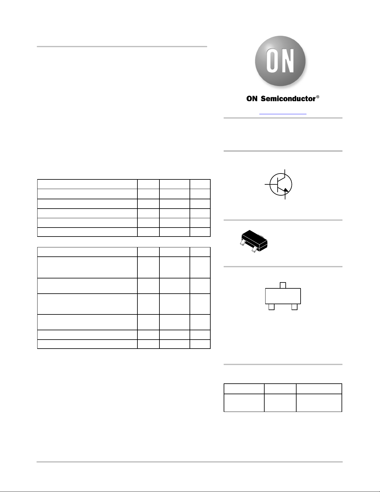
COLLECTOR
3
1
BASE
2
EMITTER
30 VOLTS, 2.0 AMPERES
NPN TRANSISTOR
SOT−23 (TO−236)
CASE 318
STYLE 6
3
2
1
3000/Tape & Ree
l
MMBT489LT1G SOT−23
(Pb−Free)
*Date Code orientation and/or overbar may
vary depending upon manufacturing location.
1
N3 M G
G
N3 = Specific Device Code
M = Date Code*
G = Pb−Free Package
(Note: Microdot may be in either location)
MARKING DIAGRAM
†For information on tape and reel specifications,
including part orientation and tape sizes, please
refer to our Tape and Reel Packaging Specification
s
Brochure, BRD8011/D.
www.onsemi.com
页面指南