下载

© Semiconductor Components Industries, LLC, 2001
October, 2016 − Rev. 14
1 Publication Order Number:
NTR1P02LT1/D
NTR1P02L, NVTR01P02L
Power MOSFET
−20 V, −1.3 A, P−Channel
SOT−23 Package
These miniature surface mount MOSFETs low R
DS(on)
assure
minimal power loss and conserve energy, making these devices ideal
for use in space sensitive power management circuitry. Typical
applications are DC−DC converters and power management in
portable and battery−powered products such as computers, printers,
PCMCIA cards, cellular and cordless telephones.
Features
• Low R
DS(on)
Provides Higher Efficiency and Extends Battery Life
• Miniature SOT−23 Surface Mount Package Saves Board Space
• NVTR Prefix for Automotive and Other Applications Requiring
Unique Site and Control Change Requirements; AEC−Q101
Qualified and PPAP Capable
• Pb−Free and Halide−Free Packages are Available
MAXIMUM RATINGS (T
J
= 25°C unless otherwise noted)
Rating Symbol Value Unit
Drain−to−Source Voltage V
DSS
−20 V
Gate−to−Source Voltage − Continuous V
GS
±12 V
Drain Current
− Continuous @ T
A
= 25°C
− Pulsed Drain Current (t
p
≤ 10 ms)
I
D
I
DM
−1.3
−4.0
A
A
Total Power Dissipation @ T
A
= 25°C P
D
400 mW
Operating and Storage Temperature Range T
J
, T
stg
− 55 to
150
°C
Thermal Resistance − Junction−to−Ambient
R
q
JA
300 °C/W
Maximum Lead Temperature for Soldering
Purposes, (1/8″ from case for 10 s)
T
L
260 °C
Stresses exceeding those listed in the Maximum Ratings table may damage the
device. If any of these limits are exceeded, device functionality should not be
assumed, damage may occur and reliability may be affected.
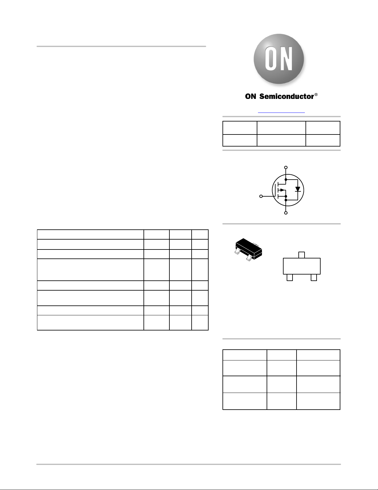
D
G
S
Device Package Shipping
†
ORDERING INFORMATION
P−Channel
†For information on tape and reel specifications,
including part orientation and tape sizes, please
refer to our Tape and Reel Packaging Specification
s
Brochure, BRD8011/D.
NTR1P02LT3G SOT−23
(Pb−Free)
10,000 Tape &
Reel
−20 V
220 mW @ −4.5 V
R
DS(on)
Max
−1.3 A
I
D
MaxV
(BR)DSS
SOT−23
CASE 318
STYLE 21
MARKING DIAGRAM &
PIN ASSIGNMENT
2
P02 = Specific Device Code
M = Date Code*
G = Pb−Free Package
1
3
NTR1P02LT1G SOT−23
(Pb−Free)
3000 Tape & Ree
l
(Note: Microdot may be in either location)
*Date Code orientation may vary depending
upon manufacturing location.
P02 M G
G
1
Gate
2
Source
Drain
3
NVTR01P02LT1G SOT−23
(Pb−Free)
3000 Tape & Ree
l
www.onsemi.com
页面指南


