
下载
© Semiconductor Components Industries, LLC, 2014
September, 2014 − Rev. 9
1 Publication Order Number:
NTD20N06/D
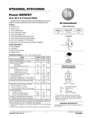
NTD20N06, NTDV20N06
Power MOSFET
20 A, 60 V, N−Channel DPAK
Designed for low voltage, high speed switching applications in power
supplies, converters and power motor controls and bridge circuits.
Features
• Lower R
DS(on)
• Lower V
DS(on)
• Lower Capacitances
• Lower Total Gate Charge
• Lower and Tighter V
SD
• Lower Diode Reverse Recovery Time
• Lower Reverse Recovery Stored Charge
• AEC Q101 Qualified − NTDV20N06
• These Devices are Pb−Free and are RoHS Compliant
Typical Applications
• Power Supplies
• Converters
• Power Motor Controls
• Bridge Circuits
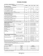
MAXIMUM RATINGS (T
J
= 25°C unless otherwise noted)
Rating
Symbol Value Unit
Drain−to−Source Voltage V
DSS
60 Vdc
Drain−to−Gate Voltage (R
GS
= 10 MW)
V
DGR
60 Vdc
Gate−to−Source Voltage
− Continuous
− Non−repetitive (t
p
v10 ms)
V
GS
V
GS
±20
±30
Vdc
Drain Current
− Continuous @ T
A
= 25°C
− Continuous @ T
A
= 100°C
− Single Pulse (t
p
v10 ms)
I
D
I
D
I
DM
20
10
60
Adc
Apk
Total Power Dissipation @ T
A
= 25°C
Derate above 25°C
Total Power Dissipation @ T
A
= 25°C (Note 1)
Total Power Dissipation @ T
A
= 25°C (Note 2)
P
D
60
0.40
1.88
1.36
W
W/°C
W
W
Operating and Storage Temperature Range T
J
, T
stg
−55 to
175
°C
Single Pulse Drain−to−Source Avalanche
Energy − Starting T
J
= 25°C
(V
DD
= 25 Vdc, V
GS
= 10 Vdc,
L = 1.0 mH, I
L
(pk) = 18.4 A, V
DS
= 60 Vdc)
E
AS
170 mJ
Thermal Resistance
− Junction−to−Case
− Junction−to−Ambient (Note 1)
− Junction−to−Ambient (Note 2)
R
q
JC
R
q
JA
R
q
JA
2.5
80
110
°C/W
Maximum Lead Temperature for Soldering
Purposes, 1/8″ from case for 10 seconds
T
L
260 °C
Stresses exceeding those listed in the Maximum Ratings table may damage the
device. If any of these limits are exceeded, device functionality should not be
assumed, damage may occur and reliability may be affected.
1. When surface mounted to an FR4 board using the minimum recommended
pad size.
2. When surface mounted to an FR4 board using the 0.5 sq in drain pad size.
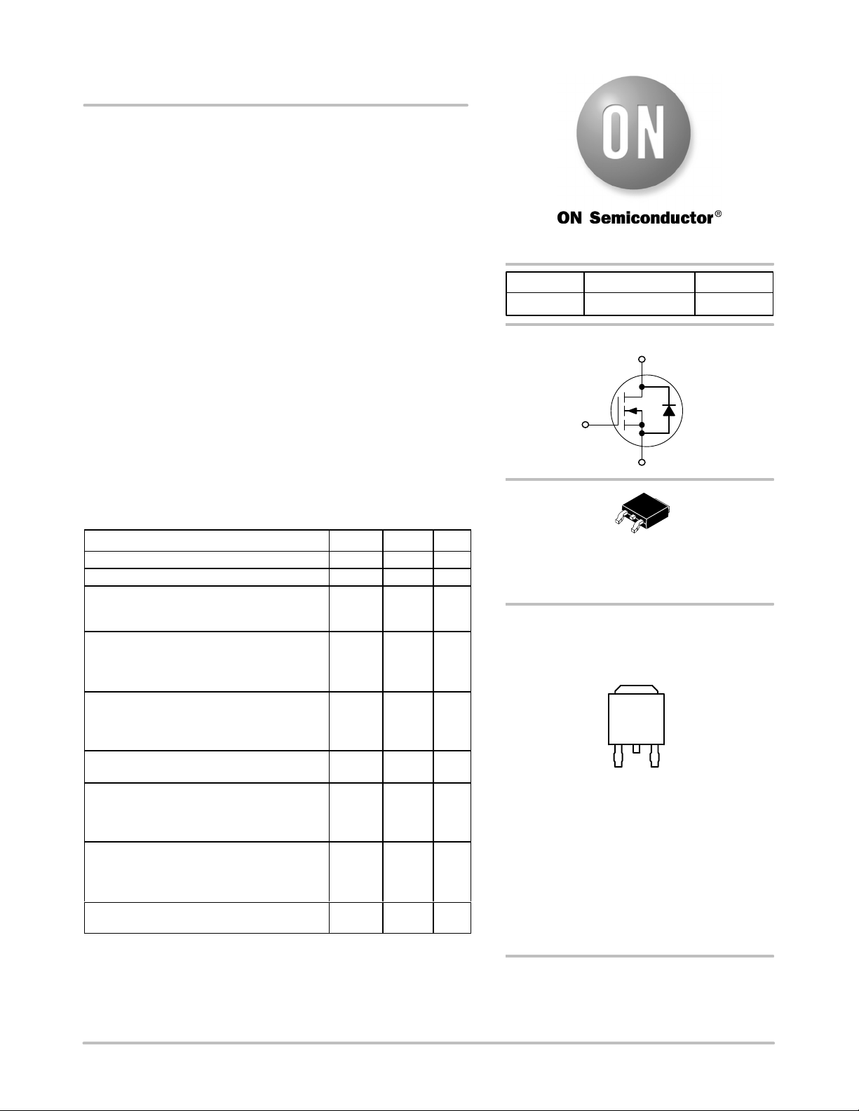
N−Channel
D
S
G
60 V
37.5 mW
R
DS(on)
TYP
20 A
I
D
MAXV
(BR)DSS
1
Gate
3
Source
2
Drain
4
Drain
DPAK
CASE 369C
STYLE 2
A = Assembly Location*
20N06 = Device Code
Y = Year
WW = Work Week
G = Pb−Free Package
1
2
3
4
MARKING DIAGRAM
& PIN ASSIGNMENTS
AYWW
20N06G
See detailed ordering and shipping information on page 2 o
f
this data sheet.
ORDERING INFORMATION
http://onsemi.com
* The Assembly Location code (A) is front side
optional. In cases where the Assembly Location is
stamped in the package, the front side assembly
code may be blank.
页面指南