
下载
Semiconductor Components Industries, LLC, 2003
March, 2003 - Rev. 3
1 Publication Order Number:
NSBC114EDXV6/D
NSBC114EDXV6T1,
NSBC114EDXV6T5
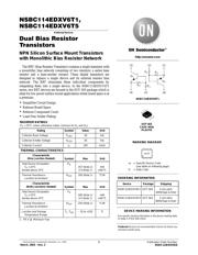
Preferred Devices
Dual Bias Resistor
Transistors
NPN Silicon Surface Mount Transistors
with Monolithic Bias Resistor Network
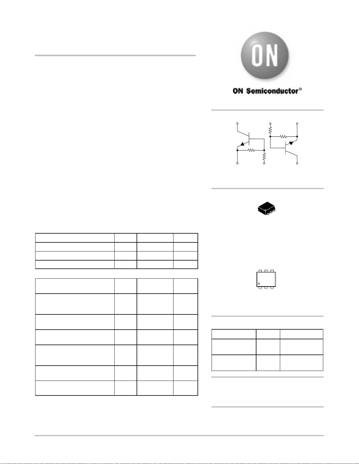
The BRT (Bias Resistor Transistor) contains a single transistor with
a monolithic bias network consisting of two resistors; a series base
resistor and a base-emitter resistor. These digital transistors are
designed to replace a single device and its external resistor bias
network. The BRT eliminates these individual components by
integrating them into a single device. In the NSBC114EDXV6T1
series, two BRT devices are housed in the SOT-563 package which is
ideal for low power surface mount applications where board space is at
a premium.
• Simplifies Circuit Design
• Reduces Board Space
• Reduces Component Count
• Lead-Free Solder Plating
MAXIMUM RATINGS
(T
A
= 25°C unless otherwise noted, common for Q
1
and Q
2
)
Rating
Symbol Value Unit
Collector-Base Voltage V
CBO
50 Vdc
Collector-Emitter Voltage V
CEO
50 Vdc
Collector Current I
C
100 mAdc
THERMAL CHARACTERISTICS
Characteristic
(One Junction Heated)
Symbol Max Unit
Total Device Dissipation
T
A
= 25°C
Derate above 25°C
P
D
357 (Note 1)
2.9 (Note 1)
mW
mW/°C
Thermal Resistance -
Junction-to-Ambient
R
JA
350 (Note 1) °C/W
Characteristic
(Both Junctions Heated)
Symbol Max Unit
Total Device Dissipation
T
A
= 25°C
Derate above 25°C
P
D
500 (Note 1)
4.0 (Note 1)
mW
mW/°C
Thermal Resistance -
Junction-to-Ambient
R
JA
250 (Note 1) °C/W
Junction and Storage
Temperature Range
T
J
, T
stg
- 55 to +150 °C
1. FR-4 @ Minimum Pad
NSBC114EDXV6T1
Preferred devices are recommended choices for future use
and best overall value.
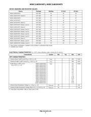
DEVICE MARKING INFORMATION
See specific marking information in the device marking table
on page 2 of this data sheet.
Q
1
R
1
R
2
R
2
R
1
Q
2
(1)(2)(3)
(4) (5) (6)
SOT-563
CASE 463A
PLASTIC
1
2
3
6
5
4
xx = Specific Device Code
(see table on following page)
D = Date Code
MARKING DIAGRAM
xx D
http://onsemi.com
Device Package Shipping
ORDERING INFORMATION
NSBC114EDXV6T1 SOT-563 4 mm pitch
4000/Tape & Reel
NSBC114EDXV6T5 SOT-563 2 mm pitch
8000/Tape & Reel