


下载
© Semiconductor Components Industries, LLC, 2013
September, 2013 − Rev. 1
1 Publication Order Number:
NJW3281/D
NJW3281G (NPN)
NJW1302G (PNP)
Complementary NPN-PNP
Silicon Power Bipolar
Transistors
The NJW3281G and NJW1302G are power transistors for high
power audio, disk head positioners and other linear applications.
Features
• Exceptional Safe Operating Area
• NPN/PNP Gain Matching within 10% from 50 mA to 5 A
• Excellent Gain Linearity
• High BVCEO
• High Frequency
• These Devices are Pb−Free and are RoHS Compliant
Benefits
• Reliable Performance at Higher Powers
• Symmetrical Characteristics in Complementary Configurations
• Accurate Reproduction of Input Signal
• Greater Dynamic Range
• High Amplifier Bandwidth
Applications
• High−End Consumer Audio Products
♦ Home Amplifiers
♦ Home Receivers
• Professional Audio Amplifiers
♦ Theater and Stadium Sound Systems
♦ Public Address Systems (PAs)
MAXIMUM RATINGS (T
J
= 25°C unless otherwise noted)
Rating
Symbol Value Unit
Collector−Emitter Voltage V
CEO
250 Vdc
Collector−Base Voltage V
CBO
250 Vdc
Emitter−Base Voltage V
EBO
5.0 Vdc
Collector−Emitter Voltage − 1.5 V V
CEX
250 Vdc
Collector Current − Continuous I
C
15 Adc
Collector Current − Peak (Note 1) I
CM
30 Adc
Base Current − Continuous I
B
1.6 Adc
Total Power Dissipation @ T
C
= 25°C
Derate Above 25°C
P
D
200
1.43
W
W/°C
Operating and Storage Junction
Temperature Range
T
J
, T
stg
− 65 to +150
°C
THERMAL CHARACTERISTICS
Characteristic Symbol Max Unit
Thermal Resistance, Junction−to−Case
R
q
JC
0.625 °C/W
Thermal Resistance, Junction−to−Ambient
R
q
JA
40 °C/W
Stresses exceeding Maximum Ratings may damage the device. Maximum
Ratings are stress ratings only. Functional operation above the Recommended
Operating Conditions is not implied. Extended exposure to stresses above the
Recommended Operating Conditions may affect device reliability.
1. Pulse Test: Pulse Width = 5 ms, Duty Cycle < 10%.
Device Package Shipping
ORDERING INFORMATION
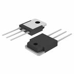
15 AMPERES
COMPLEMENTARY
SILICON POWER TRANSISTORS
250 VOLTS 200 WATTS
http://onsemi.com
NJW1302G TO−3P
(Pb−Free)
30 Units/Rail
NJW3281G TO−3P
(Pb−Free)
30 Units/Rail
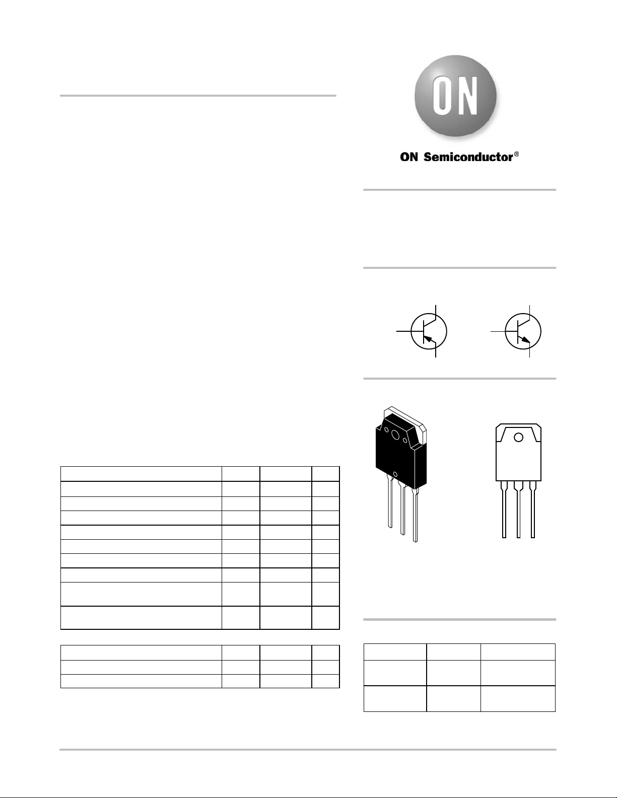
TO−3P
CASE 340AB
STYLES 1,2,3
xxxx = 0281 or 0302
G = Pb−Free Package
A = Assembly Location
Y = Year
WW = Work Week
NJWxxxG
AYWW
MARKING
DIAGRAM
1
2
3
4
123
1
BASE
EMITTER 3
COLLECTOR 2, 4
1
BASE
EMITTER 3
COLLECTOR 2, 4
PNP
NPN