
下载
© Semiconductor Components Industries, LLC, 2014
October, 2014 − Rev. 2
1 Publication Order Number:
NCV890200/D
NCV890200
2 A, 2 MHz Automotive
Buck Switching Regulator
The NCV890200 is a fixed−frequency, monolithic, Buck switching
regulator intended for Automotive, battery−connected applications
that must operate with up to a 36 V input supply. The regulator is
suitable for systems with low noise and small form factor
requirements often encountered in automotive driver information
systems. The NCV890200 is capable of converting the typical 4.5 V to
18 V automotive input voltage range to outputs as low as 3.3 V at a
constant switching frequency above the sensitive AM band,
eliminating the need for costly filters and EMI countermeasures. The
NCV890200 also provides several protection features expected in
Automotive power supply systems such as current limit, short circuit
protection, and thermal shutdown. In addition, the high switching
frequency produces low output voltage ripple even when using small
inductor values and an all−ceramic output filter capacitor − forming a
space−efficient switching regulator solution.
Features
• Internal N−Channel Power Switch
• Low V
IN
Operation Down to 4.5 V
• High V
IN
Operation to 36 V
• Withstands Load Dump to 40 V
• 2 MHz Free−running Switching Frequency
• Logic level Enable Input Can be Directly Tied to Battery
• 2.2 A (min) Cycle−by−Cycle Peak Current Limit
• Short Circuit Protection enhanced by Frequency Foldback
• ±1.75% Output Voltage Tolerance
• Output Voltage Adjustable Down to 0.8 V
• 1.4 Millisecond Internal Soft−Start
• Thermal Shutdown (TSD)
• Low Shutdown Current
• NCV Prefix for Automotive and Other Applications
Requiring Unique Site and Control Change
Requirements; AEC−Q100 Qualified and PPAP
Capable
• These Devices are Pb−Free and are RoHS Compliant
Applications
• Audio
• Infotainment
• Safety − Vision Systems
• Instrumentation
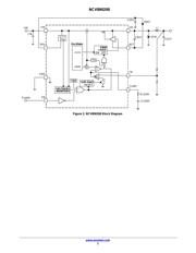
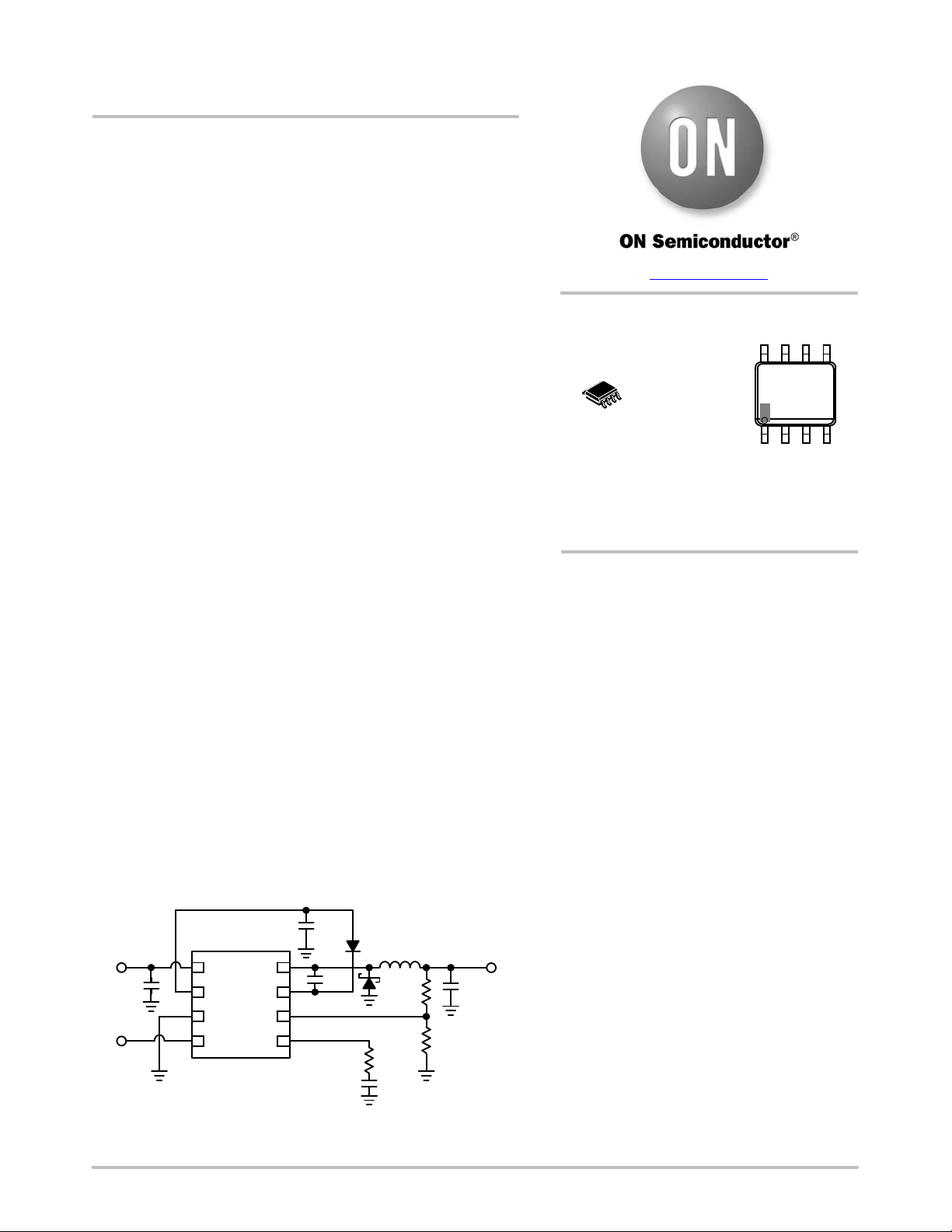
VIN
DRV
GND
EN
SW
BST
FB
COMP
VIN
EN
VOUT
CIN
CBST
DBST
DFW
RCOMP
CCOMP
COUT
L1
CDRV
NCV890200
RFB2
RFB1
1
2
3
45
6
7
8
Figure 1. Typical Application
MARKING
DIAGRAM
A = Assembly Location
L = Wafer Lot
Y = Year
W = Work Week
G = Pb−Free Device
See detailed ordering and shipping information in the package
dimensions section on page 17 of this data sheet.
ORDERING INFORMATION
SOIC−8 EP
CASE 751AC
1
8
1
8
NCV890200
ALYWX
G
www.onsemi.com
页面指南