


下载
© Semiconductor Components Industries, LLC, 2009
September, 2009 − Rev. 20
1 Publication Order Number:
MC7800/D
MC7800, MC7800A,
MC7800AE, NCV7800
1.0 A Positive Voltage
Regulators
These voltage regulators are monolithic integrated circuits designed
as fixed−voltage regulators for a wide variety of applications
including local, on−card regulation. These regulators employ internal
current limiting, thermal shutdown, and safe−area compensation. With
adequate heatsinking they can deliver output currents in excess of
1.0 A. Although designed primarily as a fixed voltage regulator, these
devices can be used with external components to obtain adjustable
voltages and currents.
Features
• Output Current in Excess of 1.0 A
• No External Components Required
• Internal Thermal Overload Protection
• Internal Short Circuit Current Limiting
• Output Transistor Safe−Area Compensation
• Output Voltage Offered in 1.5%, 2% and 4% Tolerance
• Available in Surface Mount D
2
PAK−3, DPAK−3 and Standard
3−Lead Transistor Packages
• NCV Prefix for Automotive and Other Applications Requiring Site
and Control Changes
• Pb−Free Packages are Available
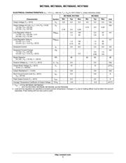
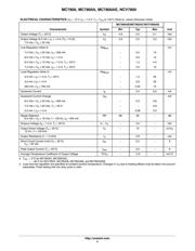
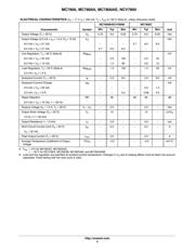
MAXIMUM RATINGS (T
A
= 25°C, unless otherwise noted)
Rating Symbol
Value Unit
369C 221A 936
Input Voltage (5.0 − 18 V)
(24 V)
V
I
35
40
Vdc
Power Dissipation P
D
Internally Limited W
Thermal Resistance,
Junction−to−Ambient
R
q
JA
92 65 Figure
15
°C/W
Thermal Resistance,
Junction−to−Case
R
q
JC
5.0 5.0 5.0 °C/W
Storage Junction Temperature
Range
T
stg
−65 to +150 °C
Operating Junction Temperature T
J
+150 °C
Stresses exceeding Maximum Ratings may damage the device. Maximum
Ratings are stress ratings only. Functional operation above the Recommended
Operating Conditions is not implied. Extended exposure to stresses above the
Recommended Operating Conditions may affect device reliability.
*This device series contains ESD protection and exceeds the following tests:
Human Body Model 2000 V per MIL_STD_883, Method 3015.
Machine Model Method 200 V.
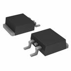
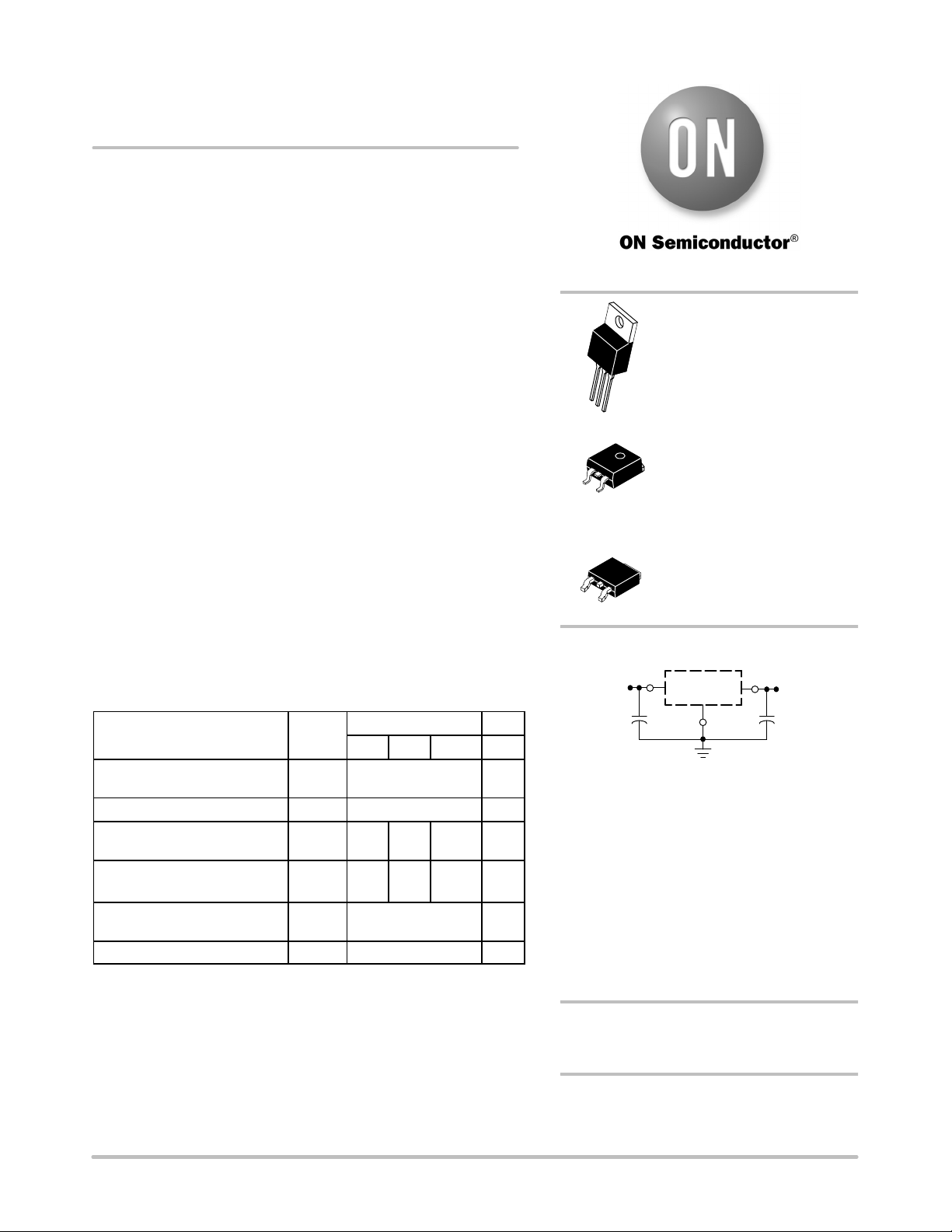
TO−220−3
T SUFFIX
CASE 221AB
1
D
2
PAK−3
D2T SUFFIX
CASE 936
2
3
See detailed ordering and shipping information in the package
dimensions section on page 23 of this data sheet.
ORDERING INFORMATION
Heatsink surface
connected to Pin 2.
Pin 1. Input
2. Ground
3. Output
Heatsink surface (shown as terminal 4 in
case outline drawing) is connected to Pin 2.
1
3
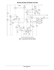
STANDARD APPLICATION
A common ground is required between the
input and the output voltages. The input voltage
must remain typically 2.0 V above the output
voltage even during the low point on the input
ripple voltage.
XX,
MC78XX
Input
C
in
*
0.33 mF
C
O
**
Output
These two digits of the type number
indicate nominal voltage.
C
in
is required if regulator is located an
appreciable distance from power supply
filter.
C
O
is not needed for stability; however,
it does improve transient response. Values
of less than 0.1 mF could cause instability.
*
**
See general marking information in the device marking
section on page 30 of this data sheet.
DEVICE MARKING INFORMATION
DPAK−3
DT SUFFIX
CASE 369C
http://onsemi.com
1
2
3
4
页面指南