

下载
© Semiconductor Components Industries, LLC, 2013
May, 2013 − Rev. 3
1 Publication Order Number:
AND8404/D
AND8404
AMIS-3062x and NCV70627
Micro-Stepping Motor
Driver Family, Robust
Motion Control Using the
AMIS-3062x and NCV70627
Introduction
The AMIS−3062x and NCV70627 is a family of
integrated micro−stepping stepper motor driver solutions
which are designed with a number of innovative features,
including a position controller as well as the control/
diagnostics interface. A number of devices in this product
family are targeted at dedicated mechatronics applications,
whereby they are coupled to a remote LIN master.
Alternatively, other versions of these devices can be
interfaced to an external microcontroller via an I
2
C bus.
In these applications, the motor driver IC receives
positioning instructions via the bus (LIN or I
2
C) and
subsequently drives the motor coils to the desired position.
The on−chip position controller is configurable (OTP) for
different motor types and positioning ranges, as well as speed,
acceleration and deceleration parameters, respectively. In
addition, the “micro−stepping” feature allows for silent
motor operation and increased positioning resolution.
The AMIS−3062x and NCV70627 family is fully
compatible with the operating voltages in automotive and
industrial systems.
This article provides guidelines for arriving at a set of
robust motion parameters for the AMIS−3062x and
NCV70627 stepper motor drivers. In this context, robust
motion control implies reducing the occurrences of
step−loss as well as false step−loss flags.
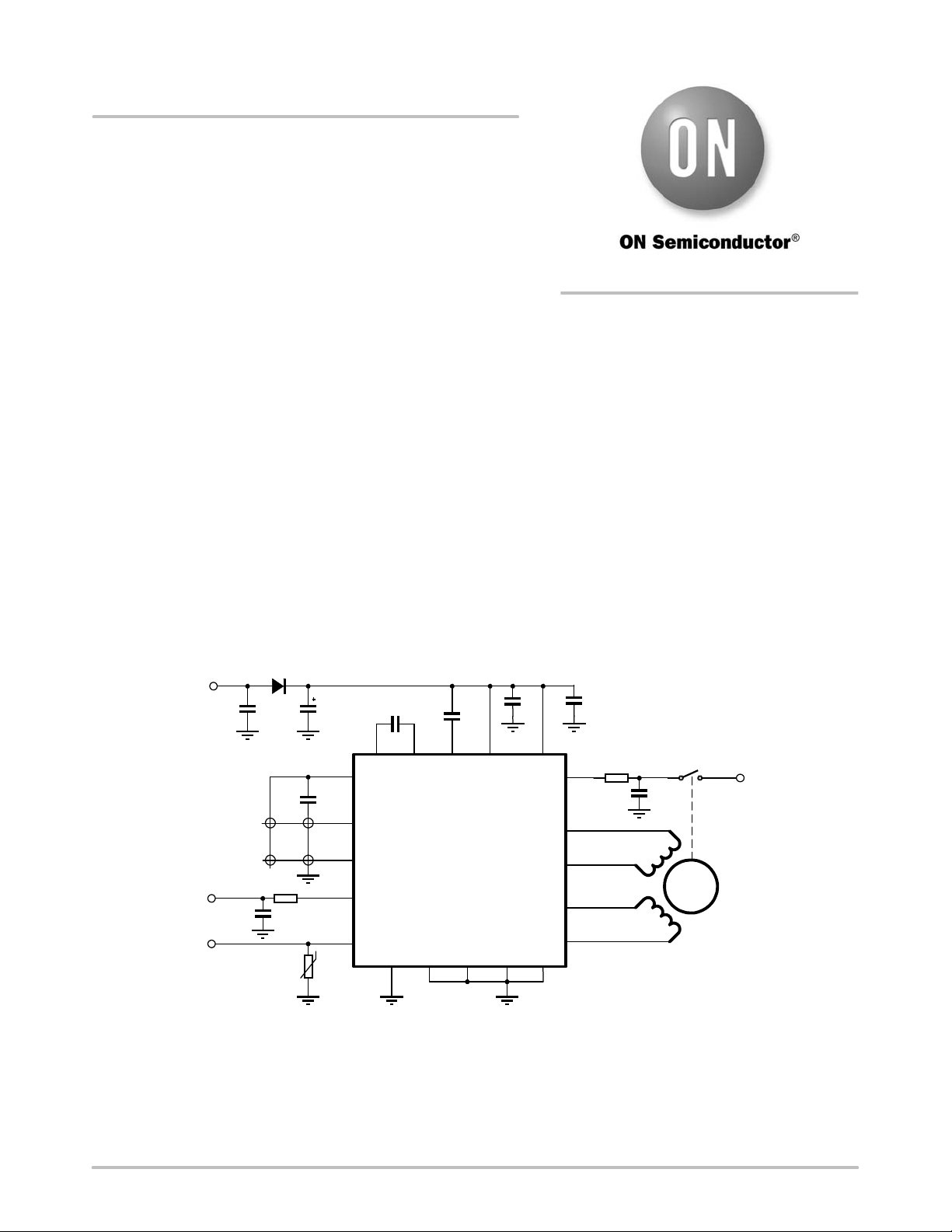
Typical Application
The typical application diagram for AMIS−30621 is
shown in Figure 1. Here, SWI is the position switch input.
If not used, Pin 20 should be left open. HW2 is an external
address pin capable of withstanding high voltage transients.
If not used, this pin should be connected to ground via a 1 kW
resistor.
AMIS−30621
V
BAT
GND
2
MOTXP
LIN
100 nF
LIN bus
2,7 nF
MOTXN
MOTYP
MOTYN
11
VDD
VBB
12
VCP
SWI
CPP
CPN
9
8
HW0
HW1
10
HW2
18
M
16
15
13
20
TST
3
VBB
19
1
6
5
47
14
17
100 nF
100 nF
220 nF
2,7 nF
220 nF
1 kW
Connect
to V
BAT
or GND
Connect
to V
BAT
or GND
1 kW
100 mF
VDR 27V
C
1
C
2
C
3
C
4
C
5
C
6
C
7
C
8
C
9
Figure 1. Typical Application Diagram
1. All resistors are 1/4 W, ± 5%.
2. C
1
, C
2
: Minimum value is 2.7 nF, maximum value is 10 nF.
3. Depending on the application, the ESR value and operating voltage of C
7
must be carefully chosen.
4. C
3
and C
4
must be close to Pins VBB and GND.
5. C
5
and C
6
must be as close as possible to Pins CPN, CPP, VCP, and VBB to reduce EMC radiation.
6. HW0 and HW1 are to be connected to VDD or GND, respectively.
http://onsemi.com
APPLICATION NOTE