
Semiconductor Components Industries, LLC, 2010
November, 2010 -- Rev . 4
1 Publication Order Number:
NCP5392/D
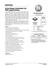
NCP5392
2/3/4--Phase Controller for
CPU Applications
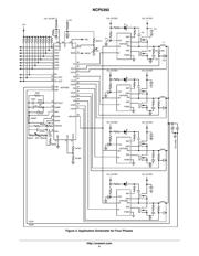
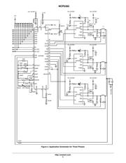
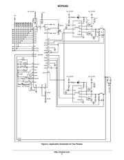
The NCP5392 provides up t o a four--phase buc k solution which
combines differential volt age sensing, differential phase current
sensing, and adaptive voltage positioning to provide accurately
regulated power for both Intel and AMD processors. Dual--edge
pulse--width modulation (PWM) combine d with inductor current
sensing reduces system cost by providing the fastest initial response
to dynamic load events. Dual --edge multiphase modulation reduces
the total bulk and ceramic output capacitance required to meet
transient regulation specifications.
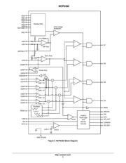
A high performance ope rational error amplifier is provided to
simplify compensation of the system. Dynamic Reference Injection
further simplifies loop compensation by eliminating the need to
compromise between closed--loop transient response and Dynamic
VID performance.
Features
Meets Intel’s VR11.1 Specifications
Meets AMD 6 Bit Code Specifications
Dual --edge PWM for Fastest Initial Response t o Transient Loading
High Performance Operational Error Amplifier
Internal Soft Start
Dynamic Refe rence Inj ection
DAC Range from 0.375 V to 1.6 V
DAC Feed Forward
0.5% DAC Voltage Accuracy from 1.0 V to 1.6 V
True Differential Remote Voltage Sensing Amplifier
Phase--to--Phase Current Balancing
“Lossless” Differential Inductor Current Sensing
Differential Current Sense Amplifiers for each Phase
Adaptive Voltage Positioning (AVP)
Oscillator Frequency Range of 100 kHz – 1 MHz
Latched Ove r Voltage Protection (OVP)
Guaranteed Startup into Pre--Charged Loads
Threshold Sensitive Enable Pin for VTT Sensing
Power Good Output with Internal Delays
Thermally Compensated Current Monitoring
This is a Pb--Free Device
Applications
Desktop Processors
40 PIN QFN, 6x6
MN SUFFIX
CASE 488AR
Device Package Shipping
†
ORDERING INFORMATION
NCP5392MNR2G* QFN--40
(Pb--Free)
2500/Tape & Reel
MARKING
DIAGRAM
NCP5392 = Specific Device Code
A = Assembly Location
WL = Wafer Lot
YY = Year
WW = Work Week
G = Pb--Free Package
NCP5392
AWLYYWWG
1
http://onsemi.com
†For information on tape and reel specifications,
including part orientation and tape sizes, please
refer to our Tape and Reel Packaging Specification
Brochure, BRD8011/D.
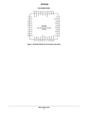
*Pin 41 is the thermal pad on the bottom of the device.
*Temperature Range: 0Cto85C
401
页面指南