
下载
© Semiconductor Components Industries, LLC, 2015
May, 2015 - Rev. 0
1 Publication Order Number:
AND9208/D
AND9208/D
Standby Power Performance
of NCP1256
The NCP1256 has been optimized to improve converter
efficiency in light−load conditions but also in no−load
situations. By reducing internal bias currents as output
power goes down, the part consumption decreases
significantly, allowing extremely low standby power
consumption figures despite the absence of high−voltage
start−up current source. When brown−out sensing takes
advantage of the X2 discharge resistors, the part gives
excellent results as we will see.
Sources of Power Waste – Primary Side
A low−voltage die such as in NCP1256 needs energy to
start−up and crank the power supply. This energy usually
comes from the input mains and is stored into the V
cc
capacitor for starting up. Several tens of milliseconds after
the capacitor voltage hits the controller turn−on voltage, an
auxiliary winding takes over and self−supplies the
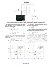
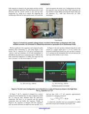
controller. A typical solution is shown in Figure 1 where
resistor R
1
forces a current I
1
from the high−voltage rail to
charge capacitor CV
cc
.
Figure 1. The Simplest Implementation to Start up
the NCP1256 from the Bulk Voltage
.
aux.
1
R
cc
CV
1CC
I
1
D
V
cc
V
bulk
1
I
2
I
5
The resistor current splits in I
2
for the capacitor but also
in I
CC1
, absorbed by the die until the V
cc
turn−on voltage is
reached. This I
CC1
current has been reduced compared to the
existing NCP125x family and is now specified at 10 mA
(max) along the whole temperature range. Assume you want
a start−up time less than 1.5 s at the lowest input voltage,
85 V rms. The V
cc
capacitor is 10 mF and the controller
turn−on voltage is 20 V (max). How much current do you
need from a 120 V bulk voltage? For the capacitor you must
deliver
I
2
u
DV @ C
Vcc
t
+
20 10u
1.5
[ 133 mA
(eq. 1)
To this value, you must add the IC own consumption of
10 mA, pushing I
2
to 145 mA with some margin. To deliver
these 145 mA from the bulk rail, resistance R
1
must be of the
following value
R
1
t
120*20
145u
+ 690 kW
(eq. 2)
Considering a normalized 680 kW resistance, a high−line
dc level on the bulk capacitor of 375 V and a 14 V operating
V
cc
, then the power permanently dissipated is
P
d
+
(375*14)
2
680k
[ 191 mW
(eq. 3)
This value may be considered low depending on the
performance you want to achieve. If you try to beat the
300 mW limit, you may have a chance to meet this number
providing the converter’s consumption is reduced at no load.
If you now want to be way less than this value, there are
several options:
1. Trade a slightly larger start−up time: by increasing
the start−up time to 3 s, the charging current drops
to 75 mA, the resistance becomes 1.3 MW and the
dissipated power drops to 100 mW.
2. Decrease the V
cc
capacitor to 4.7 mF. For instance,
increasing a little the auxiliary winding turns ratio
may improve the auxiliary V
cc
take−over time and
a 4.7 mF capacitor is enough to start up in all
conditions. In this case, you approach values
obtained with those obtained in point 1.
Besides excessive power dissipation, another drawback of
this solution is the maintaining of V
cc
a long time while the
converter has been unplugged from the mains outlet. If the
IC is latched and the user wants a quick reset, this solution
lengthens the reset time quite significantly as V
cc
does not
immediately drop to its reset value.
A second possibility is to connect the start−up resistance
to the input line directly. One of the bridge diode will ensure
half−wave rectification and the rms voltage value across the
resistance will be significantly reduced to the benefit of the
dissipated power. Figure 2 represents this solution widely
implemented in ac−dc adapters.
www.onsemi.com
APPLICATION NOTE