


© Semiconductor Components Industries, LLC, 2015
September, 2015 − Rev. 1
1 Publication Order Number:
AND9115/D
AND9115/D
NCP1255, a Controller with
Peak Output Power
Capability
The NCP1255 capitalizes on the NCP1250 circuitry to
which several enhancements have been brought.
Specifically tailored for applications requiring peak power
capability, the part can increase its switching frequency on
the fly while making sure the maximum peak current
setpoint is not exceeded. The total available power is
authorized for a period of time defined by a programmable
timer. This timer is either of full duration in an overload
situation or divided by 4 in presence of a short-circuit event.
The typical application of such a control scheme is a
converter that is thermally tailored for medium power level
while capable of delivering an extra amount of power for a
short period of time only.
Using the same protection set as NCP1250 to which a
brown-out protection has been added, the NCP1255 is the
perfect candidate when high performance, safety and cost
sensitivity are design factors.
General Description
The part is encapsulated in a SOIC−8 package but a
reduced-feature set version (no brown-out and the timer is
internally set), the NCP1254, also exists in a tiny TSOP−6
package. Featuring a low-power BiCMOS process, the die
accepts to work with V
CC
levels up to 35 V, safely clamping
the drive voltage below 12 V. With its 15 mA start-up
current, a high-value resistive network can be used in offline
applications to crank the converter, naturally minimizing the
wasted power in high-line conditions. In nominal load
operations, the switching frequency of this peak-current
mode control circuit is 65 kHz.
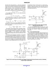
When the power demand goes up, the controller increases
the peak current setpoint until it reaches the upper limit
(0.8 V over R
sense
). At this point, the output power increase
can only be answered by further shifting the switching
frequency up until it reaches another limit, 130 kHz. The
maximum power is thus obtained at this moment. On the
contrary, in light-load operations, the part linearly reduces
its switching frequency down to 26 kHz and enters skip
cycle as power goes further down. This mode of operation
favors higher efficiency from high to moderate output levels
and ensures the lowest acoustic noise in the transformer. To
improve the EMI signature, a low-frequency modulation
brings some dither to the switching pattern. Unlike other
circuits, the dither is kept in foldback and peak excursion
modes, continuously smoothing the noise signature.
The part hosts several new protections such as an
auto-recovery brown-out circuit adjustable via a resistive
divider. A double hiccup on the V
CC
brings down the
average input power while in auto-recovery fault mode.
Regulation is ensured by pulling down the dedicated pin via
an optocoupler, driven from the secondary side by a TL431
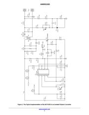
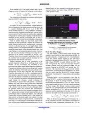
or a cheap Zener diode. Figure 1 shows the NCP1255 in its
typical implementation within a 12 V converter.
APPLICATION NOTE
www.onsemi.com