


下载

© Semiconductor Components Industries, LLC, 2014
June, 2014 − Rev. 14
1 Publication Order Number:
NBSG16VS/D
NBSG16VS
2.5 V/3.3 V SiGe Differential
Receiver/Driver with
Variable Output Swing
Description
The NBSG16VS is a differential receiver/driver targeted for high
frequency applications that require variable output swing. The device
is functionally equivalent to the EP16VS device with much higher
bandwidth and lower EMI capabilities. This device may be used for
applications driving VCSEL lasers.
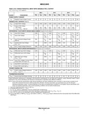
Inputs incorporate internal 50 termination resistors and accept
NECL (Negative ECL), PECL (Positive ECL), LVTTL, LVCMOS,
CML, or LVDS. The output amplitude is varied by applying a voltage
to the V
CTRL
input pin. Outputs are variable swing ECL from 100 mV
to 750 mV amplitude, optimized for operation from
V
CC
− V
EE
= 3.0 V to 3.465 V.
The V
BB
and V
MM
pins are internally generated voltage supplies
available to this device only. The V
BB
is used as a reference voltage
for single-ended NECL or PECL inputs and the V
MM
pin is used as
a reference voltage for LVCMOS inputs. For single-ended input
operation, the unused complementary differential input is connected to
V
BB
or V
MM
as a switching reference voltage. V
BB
or V
MM
may also
rebias AC-coupled inputs. When used, decouple V
BB
and V
MM
via
a 0.01 F capacitor and limit current sourcing or sinking to 0.5 mA.
When not used, V
BB
and V
MM
outputs should be left open.
Features
• Maximum Input Clock Frequency up to 12 GHz Typical
• Maximum Input Data Rate up to 12 Gb/s Typical
• 40 ps Typical Rise and Fall Times (V
CTRL
= V
CC
− 1 V)
• 120 ps Typical Propagation Delay (V
CTRL
= V
CC
− 1 V)
• Variable Swing PECL Output with Operating Range:
V
CC
= 2.375 V to 3.465 V with V
EE
= 0 V
• Variable Swing NECL Output with NECL Inputs with
Operating Range: V
CC
= 0 V with V
EE
= −2.375 V to −3.465 V
• Output Level (100 mV to 750 mV Peak-to-Peak Output;
V
CC
− V
EE
= 3.0 V to 3.465 V), Differential Output Only
• 50 Internal Input Termination Resistors
• Compatible with Existing 2.5 V/3.3 V EP Devices
• V
BB
and V
MM
Reference Voltage Output
• These are Pb-Free Devices
A = Assembly Location
L = Wafer Lot
Y = Year
W = Work Week
G = Pb-Free Package
MARKING DIAGRAMS*
http://onsemi.com
*For additional marking information, refer to
Application Note AND8002/D.
See detailed ordering and shipping information in the package
dimensions section on page 12 of this data sheet.
ORDERING INFORMATION
(Note: Microdot may be in either location)
16
SG
16VS
ALYWG
G
1
ÇÇÇ
ÇÇÇ
ÇÇÇ
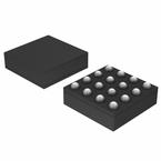
QFN−16
MN SUFFIX
CASE 485G
1
页面指南