

下载
© Semiconductor Components Industries, LLC, 2011
May, 2011 − Rev. 0
1 Publication Order Number:
NB3N3010B/D
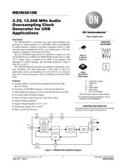
NB3N3010B
3.3V, 12.288 MHz Audio
Oversampling Clock
Generator for USB
Applications
Description
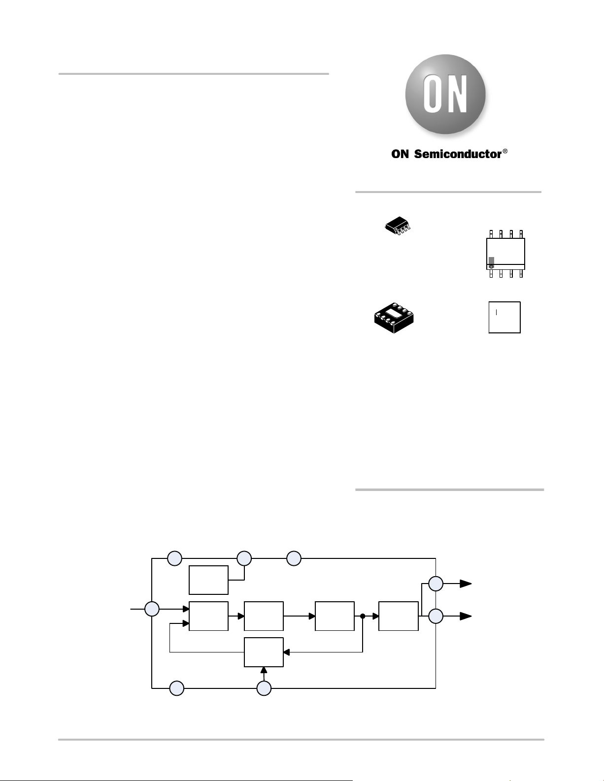
The NB3N3010B is a precision, low noise clock multiplier that
generates an output frequency of 12.288 MHz. This is accomplished
by using Frequency−Locked−Loop (FLL) techniques where a 4 kHz
reference input is multiplied by 3072, or an 8 kHz input by 1536. The
frequency multiplier is selected by the S0 pin.
The two LVCMOS output drivers are disabled to a logic Low with
the ENABLEn pin set HIGH. The NB3N3010B operates from a single
+3.3 V supply, and is available in the SOIC−8 pin package, and
optionally in a DFN8 package. The operating temperature range is
from 0°C to +85°C.
The NB3N3010B device provides the optimum combination of low
cost, flexibility, and high performance. This makes it ideal for
applications such as oversampling A−to−D and D−to−A converters
from a low reference frequency, such as a USB start−of−frame (SOF)
pulse.
Features
• Accepts 8 kHz or 4 kHz Reference Input Derived from USB
Start−of−Frame
• Generates 12.288 MHz Frequency−Locked to the Reference
• Fully Integrated Frequency−Lock−Loop with Internal Loop Filter
• Low Skew Dual LVCMOS Outputs
• Very Low Phase Noise Preserves Codec Noise Floor
• Internal Voltage Regulator
• Supply Voltage Required: +3.3 V $5%
• Temperature Range: 0°C to +85°C
• These are Pb−Free Devices
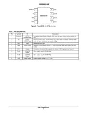
8 4
2
Tolerant
Frequency
Detector
Loop Filter
Frequency
Generator
Output
Buffers
7
Divider
3
REF
S0
CLK_B
VDD GND
1
ENABLEn
+1.8 V
Linear
Regulator
5
CFILT
CLK_A
6
Figure 1. NB3N3010B Simplified Diagram
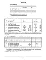
*For additional marking information, refer to
Application Note AND8002/D.
MARKING
DIAGRAMS*
SOIC−8
D SUFFIX
CASE 751
1
8
See detailed ordering and shipping information in the package
dimensions section on page 7 of this data sheet.
ORDERING INFORMATION
http://onsemi.com
3010B
ALYW
G
1
8
DFN8
MN SUFFIX
CASE 506AA
XX M G
G
14
(Note: Microdot may be in either location)
A = Assembly Location
L = Wafer Lot
Y = Year
W = Work Week
M = Date Code
G = Pb−Free Package
页面指南