


下载

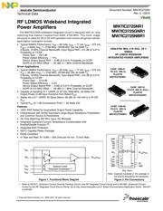
MW7IC2725NR1 MW7IC2725GNR1 MW7IC2725NBR1
1
RF Device Data
Freescale Semiconductor
RF LDMOS Wideband Integrated
Power Amplifiers
The MW7IC2725N wideband integrated circuit is designed with on- chip
matching that makes it usable from 2300- 2700 MHz. This multi- stage
structure is rated for 26 to 32 Volt operation and covers all typical cellular
base station modulation formats.
• Typical WiMAX Performance: V
DD
= 28 Volts, I
DQ1
= 77 mA, I
DQ2
= 275 mA,
P
out
= 4 Watts Avg., f = 2700 MHz, OFDM 802.16d, 64 QAM
3
/
4
,
4 Bursts, 10 MHz Channel Bandwidth, Input Signal PAR = 9.5 dB @ 0.01%
Probability on CCDF.
Power Gain — 28.5 dB
Power Added Efficiency — 17%
Device Output Signal PAR — 9 dB @ 0.01% Probability on CCDF
ACPR @ 8.5 MHz Offset — -50 dBc in 1 MHz Channel Bandwidth
Driver Applications
• Typical WiMAX Performance: V
DD
= 28 Volts, I
DQ1
= 77 mA, I
DQ2
= 275 mA,
P
out
= 26 dBm Avg., f = 2700 MHz, OFDM 802.16d, 64 QAM
3
/
4
,
4 Bursts, 10 MHz Channel Bandwidth, Input Signal PAR = 9.5 dB @ 0.01%
Probability on CCDF.
Power Gain — 27.8 dB
Power Added Efficiency — 3.2%
Device Output Signal PAR — 9 dB @ 0.01% Probability on CCDF
ACPR @ 8.5 MHz Offset — -56 dBc in 1 MHz Channel Bandwidth
• Capable of Handling 10:1 VSWR, @ 32 Vdc, 2600 MHz, 40 Watts CW
Output Power (3 dB Input Overdrive from Rated P
out
)
• Stable into a 5:1 VSWR. All Spurs Below -60 dBc @ 100 mW to 5 W CW
P
out
• Typical P
out
@ 1 dB Compression Point ] 25 Watts CW
Features
• 100% PAR Tested for Guaranteed Output Power Capability
• Characterized with Series Equivalent Large-Signal Impedance Parameters
and Common Source S-Parameters
• On-Chip Matching (50 Ohm Input, DC Blocked)
• Integrated Quiescent Current Temperature Compensation with
Enable/Disable Function
(1)
• Integrated ESD Protection
• 225°C Capable Plastic Package
• RoHS Compliant
• In Tape and Reel. R1 Suffix = 500 Units per 44 mm, 13 inch Reel.
1. Refer to AN1977, Quiescent Current Thermal Tracking Circuit in the RF Integrated Circuit Family and to AN1987, Quiescent Current
Control for the RF Integrated Circuit Device Family. Go to http://www.freescale.com/rf. Select Documentation/Application Notes - AN1977
or AN1987.
MW7IC2725NR1
MW7IC2725GNR1
MW7IC2725NBR1
2500-2700 MHz, 4 W AVG., 28 V
WiMAX
RF LDMOS WIDEBAND
INTEGRATED POWER AMPLIFIERS
CASE 1886-01
TO-270 WB-16
PLASTIC
MW7IC2725NR1
CASE 1887-01
TO-270 WB-16 GULL
PLASTIC
MW7IC2725GNR1
CASE 1329-09
TO-272 WB-16
PLASTIC
MW7IC2725NBR1
Document Number: MW7IC2725N
Rev. 3, 1/2010
Freescale Semiconductor
Technical Data
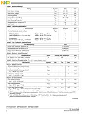
Figure 1. Functional Block Diagram
Quiescent Current
Temperature Compensation
(1)
V
DS1
RF
in
V
GS1
RF
out
/V
DS2
V
GS2
V
DS1
(Top View)
Figure 2. Pin Connections
Note: Exposed backside of the package is
the source terminal for the transistors.
GND
NC
RF
in
V
GS1
GND
RF
out
/V
DS2
GND
1
2
3
4
5
6
7
8
16
15
14
13
12
V
GS2
9
10
GND 11
V
DS1
NC
NC
NC
V
DS1
NC
NC
Freescale Semiconductor, Inc., 2008, 2010. All rights reserved.