

下载
AR
C
HIVE INF
O
RMATI
O
N
A
RCHIVE INFORMATION
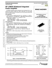
MW6IC1940GNBR1
1
RF Device Data
Freescale Semiconductor
RF LDMOS Wideband Integrated
Power Amplifier
The MW6IC1940GNB wideband integrated c ircuit is designed w ith on--chip
matching that makes it usable from 1920 to 2000 MHz. This multi-- stage
structure is rated for 26 to 32 Volt operation and covers all t y pical c ellular bas e
station modulation formats.
Final A pplication
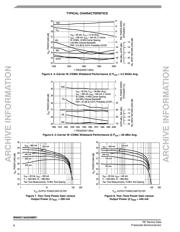
! Typical 2--Carrier W--CDMA Performance: V
DD
=28Volts,I
DQ1
= 200 mA,
I
DQ2
= 440 mA, P
out
= 4.5 Watts Avg., f = 1922.5 MHz, Channel Bandwidth =
3.84 MHz, PAR = 8.5 dB @ 0.01% Probability on CCDF.
Power Gain — 28.5 dB
Power Added Efficiency — 13.5%
IM3 @ 10 MHz Offset — --43 dBc in 3.84 MHz Bandwidth
ACPR @ 5 MHz Offset — -- 46 dBc in 3.84 MHz Bandwidth
Driver App lications
! Typical 2--Carrier W--CDMA Performance: V
DD
=28Volts,I
DQ1
= 200 mA,
I
DQ2
= 350 mA, P
out
= 26 dBm, Full Frequency Band (1920--2000 MHz),
Channel Bandwidth = 3.84 MHz, PAR = 8.5 dB @ 0.01% Probability on
CCDF.
Power Gain — 27 dB
IM3 @ 10 MHz Offset — --59 dBc in 3.84 MHz Bandwidth
ACPR @ 5 MHz Offset — -- 62 dBc in 3.84 MHz Bandwidth
! Capable of Handling 3:1 VSWR, @ 28 Vdc, 1960 MHz, 40 Watts CW
Output Power
! Stable into a 3:1 VSWR. All Spurs Below --60 dBc @ 100 mW to 20 W CW
P
out
.
Features
! Characterized with Series Equivalent Large--Signal Impedance Parameters
and Common Source Scattering Parameters
! On--Chip Matching (50 Ohm Input, DC Blocked, >3 Ohm Output)
! Integrated Quiescent Current Temperature Compensation
with Enable/Disable Function
(1)
! Integrated ESD Protection
! 225"C Capable Plastic Package
! Designed for Lower Memory Effects and Wide Instantaneous Bandwidth Applications
! RoHS Compliant
! In Tape and Reel. R1 Suffix = 500 Units per 44 mm, 13 inch Reel.
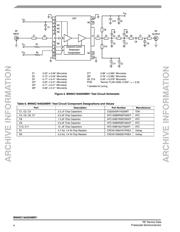
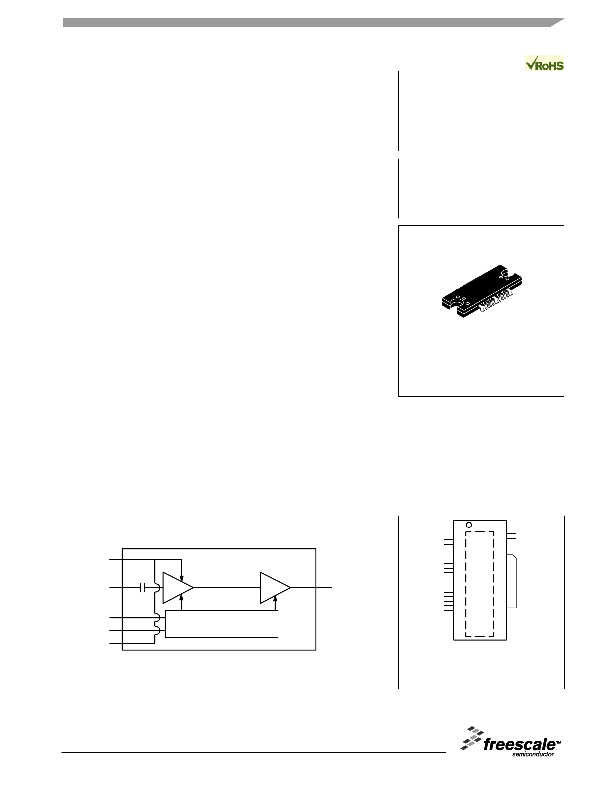
Figure 1. Functional Block Diagram Figure 2. Pin Connections
(Top View)
GND
NC
RF
in
V
GS1
GND
RF
out
/
V
DS2
GND
1
2
3
4
5
6
7
8
16
15
14
13
12
V
GS2
9
10
GND 11
Quiescent Current
Temperature Compensation
(1)
V
DS1
RF
in
V
GS1
RF
out
/V
DS2
V
GS2
V
DS1
NC
NC
NC
V
DS1
NC
NC
V
DS1
Note: Exposed backside of the package is
the source terminal for the transistors.
1. Refer to AN1977, Quiescent Current Thermal Tracking Circuit in the RF Integrated Circuit Family and to AN1987, Quiescent Current Control
for the RF Integrated Circuit Device Family. Go to http://www.freescale.com/rf. Select Documentation/Application Notes -- AN1977 or AN1987.
Document Number: MW6IC1940N--1
Rev. 3.1, 12/2009
Freescale Semiconductor
Technical Data
MW6IC1940GNBR1
1920--2000 MHz, 40 W, 28 V
2xW--CDMA
RF LDMOS WIDEBAND
INTEGRATED POWER AMPLIFIER
CASE 1329A--04
TO--272 WB--16 GULL
PLASTIC
# Freescale Semiconductor, Inc., 2006--2009.
A
ll rights reserved.