
下载
Semiconductor Components Industries, LLC, 2004
September, 2004 − Rev. 9
1 Publication Order Number:
MUN5311DW1T1/D
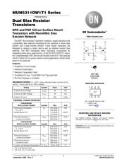
MUN5311DW1T1 Series
Preferred Devices
Dual Bias Resistor
Transistors
NPN and PNP Silicon Surface Mount
Transistors with Monolithic Bias
Resistor Network
The BRT (Bias Resistor Transistor) contains a single transistor with
a monolithic bias network consisting of two resistors; a series base
resistor and a base−emitter resistor. These digital transistors are
designed to replace a single device and its external resistor bias
network. The BRT eliminates these individual components by
integrating them into a single device. In the MUN5311DW1T1 series,
two complementary BRT devices are housed in the SOT−363 package
which is ideal for low power surface mount applications where board
space is at a premium.
Features
• Simplifies Circuit Design
• Reduces Board Space
• Reduces Component Count
• Available in 8 mm, 7 inch/3000 Unit Tape and Reel
• Pb−Free Package is Available
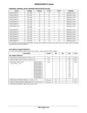
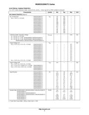
MAXIMUM RATINGS (T
A
= 25°C unless otherwise noted, common for Q
1
and Q
2
, − minus sign for Q
1
(PNP) omitted)
Rating
Symbol Value Unit
Collector-Base Voltage V
CBO
50 Vdc
Collector-Emitter Voltage V
CEO
50 Vdc
Collector Current I
C
100 mAdc
THERMAL CHARACTERISTICS
Characteristic
(One Junction Heated)
Symbol Max Unit
Total Device Dissipation
T
A
= 25°C
Derate above 25°C
P
D
187 (Note 1)
256 (Note 2)
1.5 (Note 1)
2.0 (Note 2)
mW
mW/°C
Thermal Resistance −
Junction-to-Ambient
R
JA
670 (Note 1)
490 (Note 2)
°C/W
Characteristic
(Both Junctions Heated)
Symbol Max Unit
Total Device Dissipation
T
A
= 25°C
Derate above 25°C
P
D
250 (Note 1)
385 (Note 2)
2.0 (Note 1)
3.0 (Note 2)
mW
mW/°C
Thermal Resistance −
Junction-to-Ambient
R
JA
493 (Note 1)
325 (Note 2)
°C/W
Thermal Resistance −
Junction-to-Lead
R
JL
188 (Note 1)
208 (Note 2)
°C/W
Junction and Storage Temperature T
J
, T
stg
−55 to +150 °C
1. FR−4 @ Minimum Pad
2. FR−4 @ 1.0 x 1.0 inch Pad
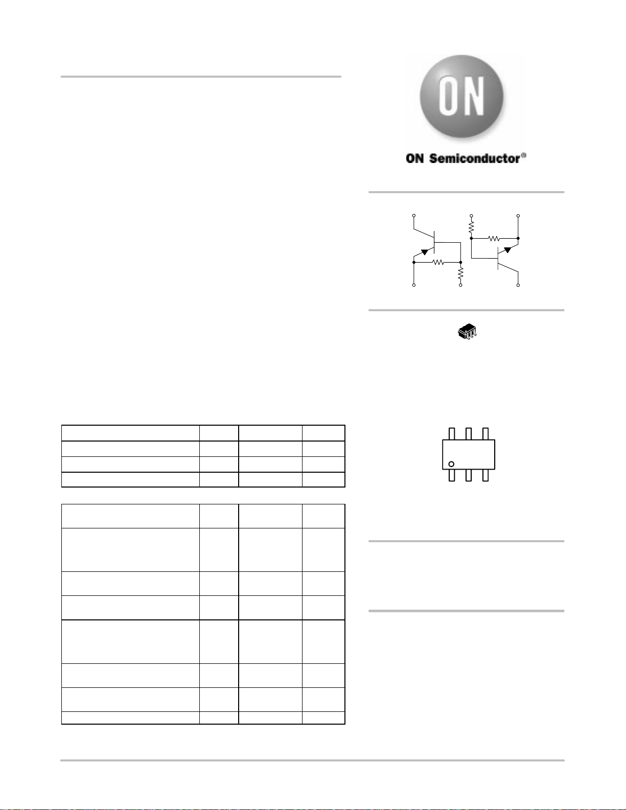
SOT−363
CASE 419B
STYLE 1
MARKING DIAGRAM
Preferred devices are recommended choices for future use
and best overall value.
ORDERING AND DEVICE MARKING
INFORMATION
See detailed ordering, shipping, and specific marking
information in the table on page 2 of this data sheet.
Q
1
R
1
R
2
R
2
R
1
Q
2
(1)(2)(3)
(4) (5) (6)
1
6
XX
d
XX= Specific Device Code
d
= Date Code
= (See Page 2)
1
6
http://onsemi.com