

下载
Products and specifications discussed herein are subject to change by Micron without notice.
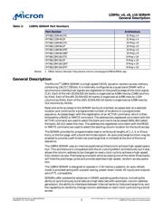
128Mb: x4, x8, x16 SDRAM
Features
PDF: 09005aef8091e66d/Source: 09005aef8091e625 Micron Technology, Inc., reserves the right to change products or specifications without notice.
128MSDRAM_1.fm - Rev. N 1/09 EN
1 ©1999 Micron Technology, Inc. All rights reserved.
SDRAM
MT48LC32M4A2 – 8 Meg x 4 x 4 banks
MT48LC16M8A2 – 4 Meg x 8 x 4 banks
MT48LC8M16A2 – 2 Meg x 16 x 4 banks
For the latest data sheet, refer to Micron’s Web site: www.micron.com
Features
• PC100- and PC133-compliant
• Fully synchronous; all signals r
egistered on positive edge
of system clock
• Internal pipelined operation; column address can be
changed every clock cycle
• Internal banks for hiding row access/precharge
• Programmable burst lengths (BL): 1, 2,
4, 8, or full page
• Auto precharge, includes concur
rent auto precharge, and
auto refresh modes
• Self refresh mode; standard and low power
• 64ms, 4,096-cycle refresh (commercial & industrial)
• 16ms, 4,096-cycle refresh (Automotive)
• LVTTL-compatible inputs and outputs
• Single +3.3 ±0.3V power supply
Options Designator
• Configurations
• Write recovery (
t
WR)
• Package/Pinout
• Timing (cycle time)
• Self refresh
•Design revision
• Operating temperature range
None
IT
3
AT
3
Notes: 1. Refer to Micron technical note: TN-48-05.
2. Off-center parting line.
3.
Consult Micron for availability.
4. x16 only.
– 32 Meg x 4 (8 Meg x 4 x 4 banks) 32M4
– 16 Meg x 8 (4 Meg x 8 x 4 banks) 16M8
– 8 Meg x 16 (2 Meg x 16 x 4 banks) 8M16
–
t
WR = “2 CLK”
1
A2
– P
lastic package – OCPL
2
– 54-pin TSOP II (400 mil) TG
– 54-pin TSOP II (400 mil) Pb-free P
– 60-ball FBGA (8mm x 16mm) FB
3
– 60-ball FBGA (8mm x 16mm) Pb-free BB
3
– 54-ball VFBGA (8mm x 8mm) F4
4
– 54-ball VFBGA (8mm x 8mm) Pb-free B4
4
– 7.5ns @ CL = 3 (PC133) -75
– 7.5ns @ CL = 2 (PC133) -7E
– 6.0ns @ CL = 3 (x16 only) -6A
– St
andard None
– Low power L
:G
– C
ommercial (0°C to +70°C)
– I
ndustrial (–40°C to +85°C)
– Automotive (–40°C to +105°C)
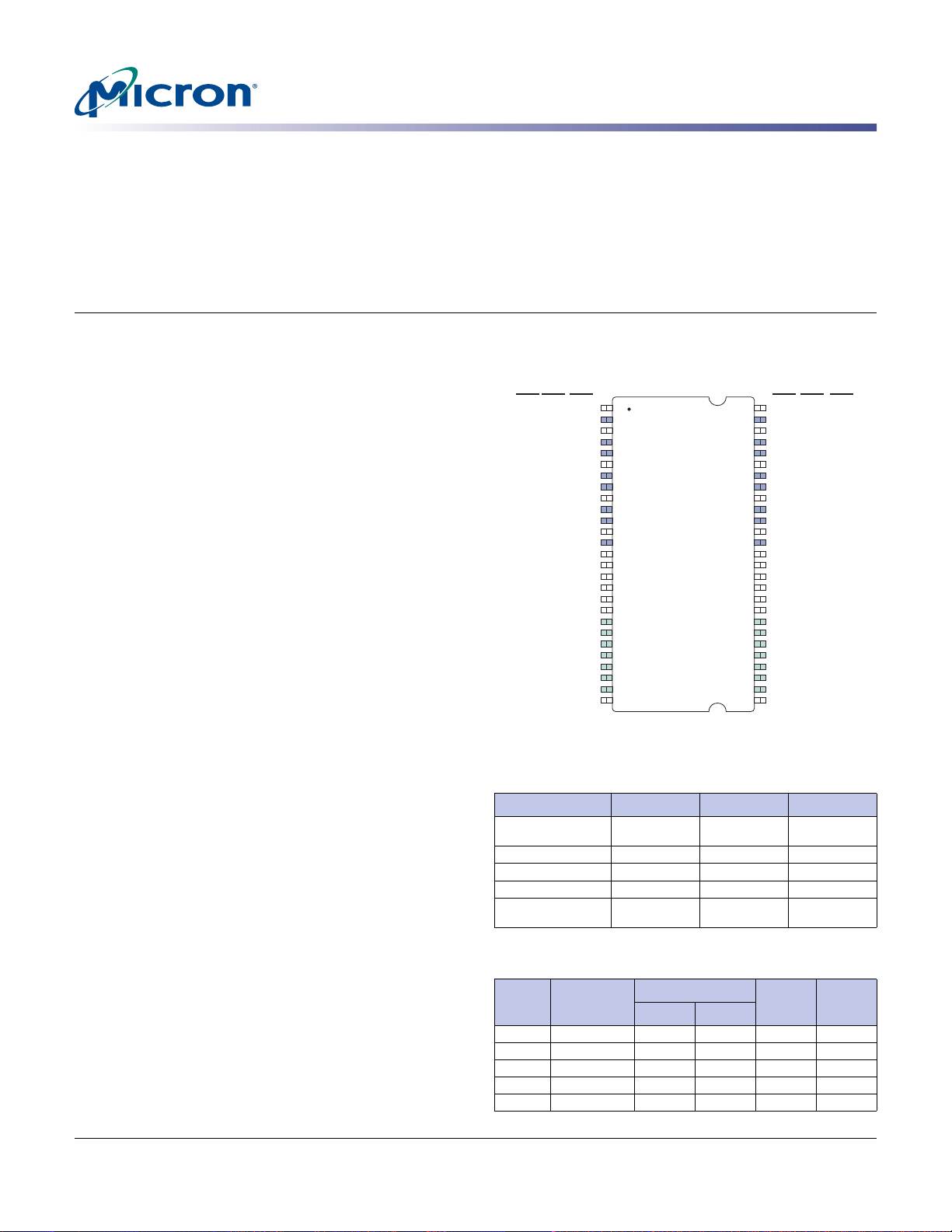
Figure 1: 54-Pin TSOP Pin Assignment
(Top View)
Notes: 1. The # symbol indicates signal is active LOW. A dash (-) indicates
x8 and x4 pin function is same as x16 pin function.
Table 1: Address Table
32 Meg x 4 16 Meg x 8 8 Meg x 16
Configuration
8 Meg x 4 x 4
banks
4 Meg x 8 x 4
banks
2 Meg x 16 x 4
banks
Refresh count
4K 4K 4K
Row addressing
4K (A0–A11) 4K (A0–A11) 4K (A0–A11)
Bank addressing
4 (BA0, BA1) 4 (BA0, BA1) 4 (BA0, BA1)
Column addressing
2K (A0–A9,
A11)
1K (A0–A9) 512 (A0–A8)
Table 2: Key Timing Parameters
CL = CAS (Read) latency
Speed
Grade
Clock
Frequency
Access Time
Setup
Time
Hold
Time
CL = 2 CL = 3
-6A 167 MHz – 5.4ns 1.5ns 0.8ns
-7E 143 MHz – 5.4ns 1.5ns 0.8ns
-7E 133 MHz 5.4ns – 1.5ns 0.8ns
-75 133 MHz – 5.4ns 1.5ns 0.8ns
-75 100 MHz 6ns – 1.5ns 0.8ns
V
DD
DQ0
V
DD
Q
DQ1
DQ2
VssQ
DQ3
DQ4
V
DD
Q
DQ5
DQ6
VssQ
DQ7
V
DD
DQML
WE#
CAS#
RAS#
CS#
BA0
BA1
A10
A0
A1
A2
A3
V
DD
1
2
3
4
5
6
7
8
9
10
11
12
13
14
15
16
17
18
19
20
21
22
23
24
25
26
27
54
53
52
51
50
49
48
47
46
45
44
43
42
41
40
39
38
37
36
35
34
33
32
31
30
29
28
Vss
DQ15
VssQ
DQ14
DQ13
V
DD
Q
DQ12
DQ11
VssQ
DQ10
DQ9
V
DD
Q
DQ8
Vss
NC
DQMH
CLK
CKE
NC
A11
A9
A8
A7
A6
A5
A4
Vss
x8x16 x16x8 x4x4
-
DQ0
-
NC
DQ1
-
NC
DQ2
-
NC
DQ3
-
NC
-
NC
-
-
-
-
-
-
-
-
-
-
-
-
-
NC
-
NC
DQ0
-
NC
NC
-
NC
DQ1
-
NC
-
NC
-
-
-
-
-
-
-
-
-
-
-
-
-
DQ7
-
NC
DQ6
-
NC
DQ5
-
NC
DQ4
-
NC
-
-
DQM
-
-
-
-
-
-
-
-
-
-
-
-
NC
-
NC
DQ3
-
NC
NC
-
NC
DQ2
-
NC
-
-
DQM
-
-
-
-
-
-
-
-
-
-
-