

下载
1
64Mb: x32 SDRAM Micron Technology, Inc., reserves the right to change products or specifications without notice.
64MSDRAMx32_5.p65 – Rev. 9/00 ©2000, Micron Technology, Inc.
64Mb: x32
SDRAM
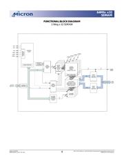
2 Meg x 32
Configuration 512K x 32 x 4 banks
Refresh Count 4K
Row Addressing 2K (A0-A10)
Bank Addressing 4 (BA0, BA1)
Column Addressing 256 (A0-A7)
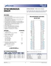
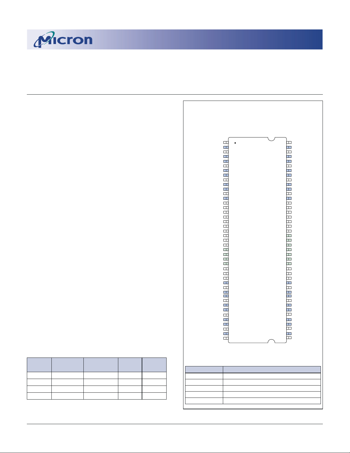
PIN ASSIGNMENT (TOP VIEW)
86-PIN TSOP
FEATURES
• PC100 functionality
• Fully synchronous; all signals registered on positive
edge of system clock
• Internal pipelined operation; column address can
be changed every clock cycle
• Internal banks for hiding row access/precharge
• Programmable burst lengths: 1, 2, 4, 8, or full page
• Auto Precharge, includes CONCURRENT AUTO
PRECHARGE, and Auto Refresh Modes
• Self Refresh Mode
• 64ms, 4,096-cycle refresh (15.6µs/row)
• LVTTL-compatible inputs and outputs
• Single +3.3V ±0.3V power supply
• Supports CAS latency of 1, 2, and 3.
OPTIONS MARKING
• Configuration
2 Meg x 32 (512K x 32 x 4 banks) 2M32B2
• Plastic Package - OCPL
1
86-pin TSOP (400 mil) TG
• Timing (Cycle Time)
5ns (200 MHz) -5
5.5ns (183 MHz) -55
6ns (166 MHz) -6
7ns (143 MHz) -7
• Operating Temperature Range
Commercial (0° to +70°C) None
Extended (-40°C to +85°C) IT
2
NOTE: 1. Off-center parting line
2. Available on -7
Part Number Example:
MT48LC2M32B2TG-7
Note: The # symbol indicates signal is active LOW.
V
DD
DQ0
V
DD
Q
DQ1
DQ2
V
SS
Q
DQ3
DQ4
V
DD
Q
DQ5
DQ6
V
SS
Q
DQ7
NC
V
DD
DQM0
WE#
CAS#
RAS#
CS#
NC
BA0
BA1
A10
A0
A1
A2
DQM2
V
DD
NC
DQ16
V
SS
Q
DQ17
DQ18
V
DD
Q
DQ19
DQ20
V
SS
Q
DQ21
DQ22
V
DD
Q
DQ23
V
DD
1
2
3
4
5
6
7
8
9
10
11
12
13
14
15
16
17
18
19
20
21
22
23
24
25
26
27
28
29
30
31
32
33
34
35
36
37
38
39
40
41
42
43
86
85
84
83
82
81
80
79
78
77
76
75
74
73
72
71
70
69
68
67
66
65
64
63
62
61
60
59
58
57
56
55
54
53
52
51
50
49
48
47
46
45
44
V
SS
DQ15
V
SS
Q
DQ14
DQ13
V
DD
Q
DQ12
DQ11
V
SS
Q
DQ10
DQ9
V
DD
Q
DQ8
NC
V
SS
DQM1
NC
NC
CLK
CKE
A9
A8
A7
A6
A5
A4
A3
DQM3
V
SS
NC
DQ31
V
DD
Q
DQ30
DQ29
V
SS
Q
DQ28
DQ27
V
DD
Q
DQ26
DQ25
V
SS
Q
DQ24
V
SS
SYNCHRONOUS
DRAM
MT48LC2M32B2 - 512K x 32 x 4 banks
For the latest data sheet, please refer to the Micron Web
site: www.micronsemi.com/datasheets/sdramds.html
KEY TIMING PARAMETERS
SPEED CLOCK ACCESS TIME SETUP HOLD
GRADE FREQUENCY CL = 3* TIME TIME
-5 200 MHz 4.5ns 1.5ns 1ns
-55 183 MHz 5ns 1.5ns 1ns
-6 166 MHz 5.5ns 1.5ns 1ns
-7 143 MHz 5.5ns 2ns 1ns
*CL = CAS (READ) latency