
šłčŤĹĹ
1
SLAA322D‚ÄďAugust 2006‚ÄďRevised July 2017
Submit Documentation Feedback
Copyright ¬© 2006‚Äď2017, Texas Instruments Incorporated
MSP430‚ĄĘ 32-kHz Crystal Oscillators
Application Report
SLAA322D‚ÄďAugust 2006‚ÄďRevised July 2017
MSP430‚ĄĘ 32-kHz Crystal Oscillators
Peter Spevak and Peter Forstner............................................................................. MSP430 Applications
ABSTRACT
Selection of the right crystal, correct load circuit, and proper board layout are important for a stable crystal
oscillator. This application report summarizes crystal oscillator function and explains the parameters to
select the correct crystal for ultra-low-power operation of an MSP430‚ĄĘ MCU. In addition, hints and
examples for correct board layout are given. The document also contains detailed information on the
possible oscillator tests to ensure stable oscillator operation in mass production.
Contents
1 The 32-kHz Crystal Oscillator.............................................................................................. 2
1.1 The Crystal .......................................................................................................... 2
1.2 The Oscillator........................................................................................................ 3
2 Crystal Selection............................................................................................................. 4
2.1 Effective Load Capacitance ....................................................................................... 4
2.2 ESR Value........................................................................................................... 5
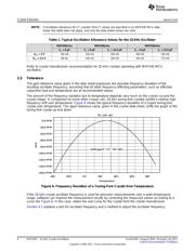
2.3 Tolerance ............................................................................................................ 6
2.4 Start-up Time........................................................................................................ 7
3 PCB Design Considerations................................................................................................ 8
4 Testing the Crystal Oscillator ............................................................................................. 10
4.1 Oscillator Frequency vs Load Capacitance.................................................................... 10
4.2 Negative Resistance Method .................................................................................... 10
4.3 Relationship Between Crystal ESR and Safety Factor....................................................... 11
5 Crystal Oscillator in Production........................................................................................... 12
5.1 PCB Material, Quality, and Cleaning ........................................................................... 12
5.2 Soldering and Contact Impedance.............................................................................. 13
5.3 Environmental Influences, Temperature, and Humidity...................................................... 13
5.4 Device-Specific Features to Support Better Start-up Behavior.............................................. 14
6 Hardware Troubleshoot for Crystal-Oscillator Start-up in Production ............................................... 18
7 References.................................................................................................................. 20
List of Figures
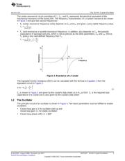
1 Mechanical Oscillation of a Tuning-Fork Crystal ........................................................................ 2
2 Equivalent Circuit of a Crystal.............................................................................................. 2
3 Reactance of a Crystal...................................................................................................... 3
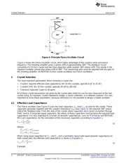
4 Principle Pierce Oscillator Circuit.......................................................................................... 4
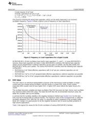
5 Frequency vs Load Capacitance for a 0-ppm Crystal .................................................................. 5
6 Frequency Deviation of a Tuning-Fork Crystal Over Temperature.................................................... 6
7 Layout Without and With External Load Capacitors (XIN and XOUT Neighboring Pins Are Standard
Function Pins)................................................................................................................ 9
8 Layout With External Capacitors and Ground Guard Ring (XIN and XOUT Neighboring Pins Are NC
Pins) Examples for MSP430F41x and MSP430F1232IRHB........................................................... 9
9 Negative Resistance Method With Added Resistor R
Q
............................................................... 11
10 XTS Toggle Assembler Code for an F4xx Device ..................................................................... 15
11 Nonoptimized PCB for General Test Purpose.......................................................................... 16