
下载
MPC9352
Rev. 6, 1/2005
Freescale Semiconductor
Technical Data
Freescale Confidential Proprietary, NDA Required / Preliminary
© Freescale Semiconductor, Inc., 2005. All rights reserved.
This document contains certain information on a new product.
Specifications and information herein are subject to change without notice.
3.3 V/2.5 V 1:11 LVCMOS Zero
Delay Clock Generator
The MPC9352 is a 3.3 V or 2.5 V compatible, 1:11 PLL based clock generator
targeted for high performance clock tree applications. With output frequencies up
to 200 MHz and output skews lower than 200 ps, the device meets the needs of
most demanding clock applications.
Features
• Configurable 11 outputs LVCMOS PLL clock generator
• Fully integrated PLL
• Wide range of output clock frequency of 16.67 MHz to 200 MHz
• Multiplication of the input reference clock frequency by 3, 2, 1, 3 ÷ 2, 2 ÷ 3,
1 ÷ 3 and 1 ÷ 2
• 2.5 V and 3.3 V LVCMOS compatible
• Maximum output skew of 200 ps
• Supports zero-delay applications
• Designed for high-performance telecom, networking and computing
applications
• 32-lead LQFP package
• 32-lead Pb-free Package Available
• Ambient Temperature Range –40°C to +85°C
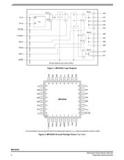
Functional Description
The MPC9352 is a fully 3.3 V or 2.5 V compatible PLL clock generator and
clock driver. The device has the capability to generate output clock signals of
16.67 to 200 MHz from external clock sources. The internal PLL is optimized for
its frequency range and does not require external lock filter components. One output of the MPC9352 has to be connected to the
PLL feedback input FB_IN to close the external PLL feedback path. The output divider of this output setting determines the PLL
frequency multiplication factor. This multiplication factor, F_RANGE, and the reference clock frequency must be selected to sit-
uate the VCO in its specified lock range. The frequency of the clock outputs can be configured individually for all three output
banks by the FSELx pins supporting systems with different, but phase-aligned, clock frequencies.
The PLL of the MPC9352 minimizes the propagation delay, and therefore, supports zero-delay applications. All inputs and out-
puts are LVCMOS compatible. The outputs are optimized to drive parallel terminated 50Ω transmission lines. Alternatively, each
output can drive up to two series terminated transmission lines giving the device an effective fanout of 22.
The device also supports output high-impedance disable and a PLL bypass mode for static system test and diagnosis. The
MPC9352 is packaged in a 32 ld LQFP.
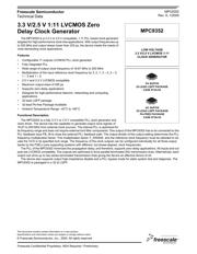
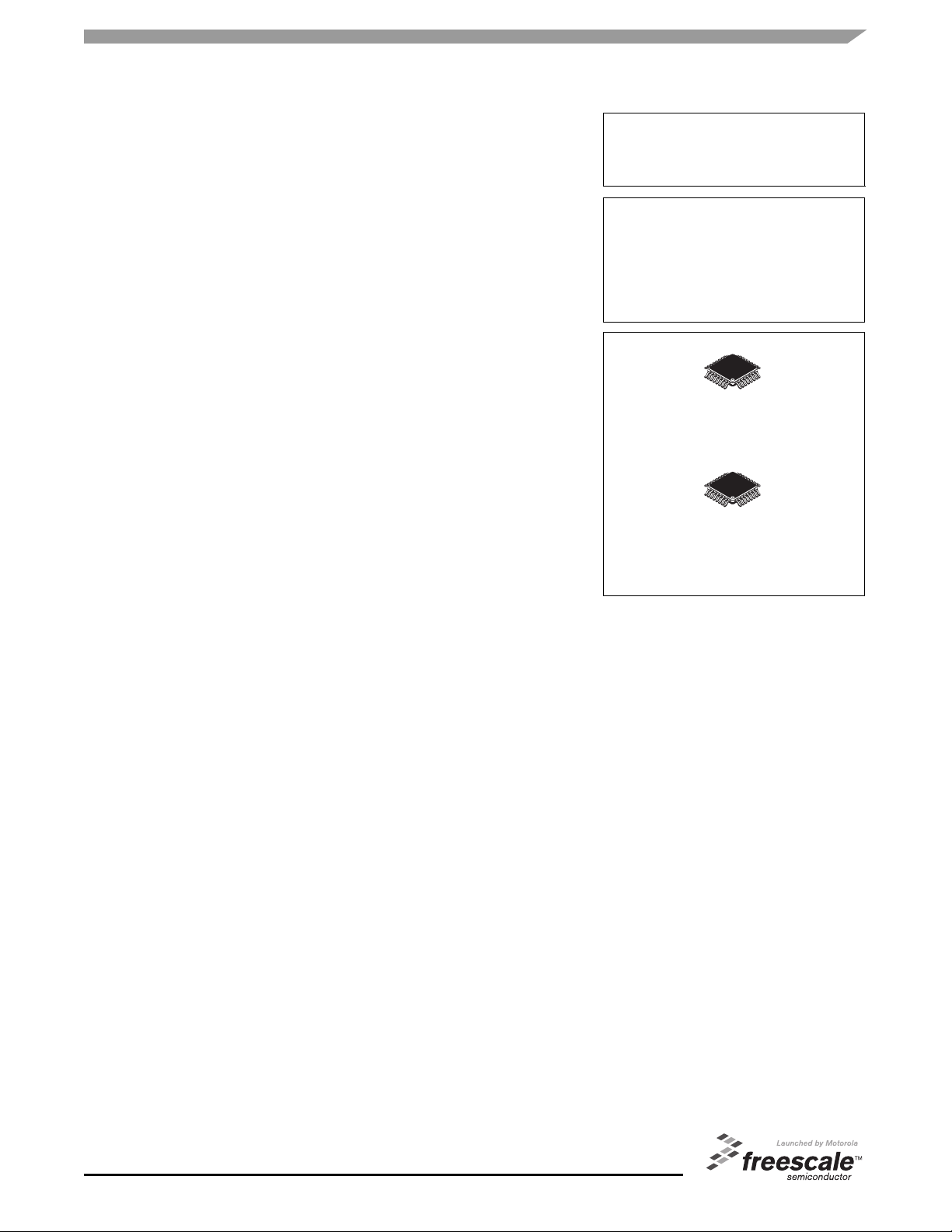
MPC9352
LOW VOLTAGE
3.3 V/2.5 V LVCMOS 1:11
CLOCK GENERATOR
FA SUFFIX
32-LEAD LQFP PACKAGE
CASE 873A-03
AC SUFFIX
32-LEAD LQFP PACKAGE
Pb-FREE PACKAGE
CASE 873A-03