


下载

Semiconductor Components Industries, LLC, 2001
November, 2001 – Rev. 2
1 Publication Order Number:
MMUN2111LT1/D
MMUN2111LT1 Series
Preferred Devices
Bias Resistor Transistors
PNP Silicon Surface Mount Transistors
with Monolithic Bias Resistor Network
This new series of digital transistors is designed to replace a single
device and its external resistor bias network. The BRT (Bias Resistor
Transistor) contains a single transistor with a monolithic bias network
consisting of two resistors; a series base resistor and a base-emitter
resistor. The BRT eliminates these individual components by
integrating them into a single device. The use of a BRT can reduce
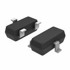
both system cost and board space. The device is housed in the SOT-23
package which is designed for low power surface mount applications.
• Simplifies Circuit Design
• Reduces Board Space
• Reduces Component Count
• The SOT-23 package can be soldered using wave or reflow. The
modified gull-winged leads absorb thermal stress during soldering
eliminating the possibility of damage to the die.
• Available in 8 mm embossed tape and reel. Use the Device Number
to order the 7 inch/3000 unit reel. Replace “T1” with “T3” in the
Device Number to order the 13 inch/10,000 unit reel.
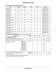
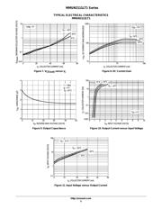
MAXIMUM RATINGS (T
A
= 25°C unless otherwise noted)
Rating
Symbol Value Unit
Collector-Base Voltage V
CBO
50 Vdc
Collector-Emitter Voltage V
CEO
50 Vdc
Collector Current I
C
100 mAdc
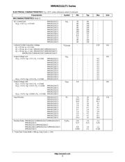
THERMAL CHARACTERISTICS
Characteristic Symbol Max Unit
Total Device Dissipation
T
A
= 25°C
Derate above 25°C
P
D
246 (Note 1.)
400 (Note 2.)
1.5 (Note 1.)
2.0 (Note 2.)
mW
°C/W
Thermal Resistance –
Junction-to-Ambient
R
θJA
508 (Note 1.)
311 (Note 2.)
°C/W
Thermal Resistance –
Junction-to-Lead
R
θJL
174 (Note 1.)
208 (Note 2.)
°C/W
Junction and Storage
Temperature Range
T
J
, T
stg
–55 to +150 °C
1. FR–4 @ Minimum Pad
2. FR–4 @ 1.0 x 1.0 inch Pad
SOT–23
CASE 318
STYLE 6
http://onsemi.com
A6x = Device Marking
x = A – L (See
Page 2)
M = Date Code
A6x M
MARKING DIAGRAM
1
3
2
Preferred devices are recommended choices for future use
and best overall value.
PIN 3
COLLECTOR
(OUTPUT)
PIN 2
EMITTER
(GROUND)
PIN 1
BASE
(INPUT)
R1
R2
DEVICE MARKING INFORMATION
See specific marking information in the device marking table
on page 2 of this data sheet.