
下载
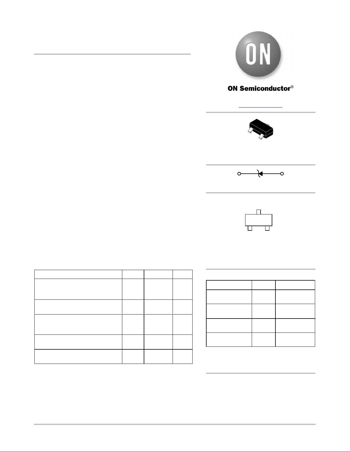
© Semiconductor Components Industries, LLC, 2001
October, 2016 − Rev. 13
1 Publication Order Number:
MMBZ5221BLT1/D
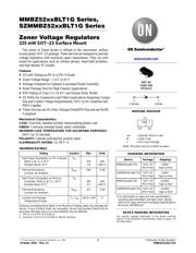
MMBZ52xxBLT1G Series,
SZMMBZ52xxBLT1G Series
Zener Voltage Regulators
225 mW SOT−23 Surface Mount
This series of Zener diodes is offered in the convenient, surface
mount plastic SOT−23 package. These devices are designed to provide
voltage regulation with minimum space requirement. They are well
suited for applications such as cellular phones, hand held portables,
and high density PC boards.
Features
• 225 mW Rating on FR−4 or FR−5 Board
• Zener Voltage Range − 2.4 V to 91 V
• Package Designed for Optimal Automated Board Assembly
• Small Package Size for High Density Applications
• ESD Rating of Class 3 (> 16 KV) per Human Body Model
• SZ Prefix for Automotive and Other Applications Requiring Unique
Site and Control Change Requirements; AEC−Q101 Qualified and
PPAP Capable
• These Devices are Pb−Free, Halogen Free/BFR Free and are RoHS
Compliant
Mechanical Characteristics
CASE:
Void-free, transfer-molded, thermosetting plastic case
FINISH: Corrosion resistant finish, easily solderable
MAXIMUM CASE TEMPERATURE FOR SOLDERING PURPOSES:
260°C for 10 Seconds
POLARITY: Cathode indicated by polarity band
FLAMMABILITY RATING: UL 94 V−0
MAXIMUM RATINGS
Rating Symbol Max Units
Total Power Dissipation on FR−5 Board,
(Note 1) @ T
A
= 25°C
Derated above 25°C
P
D
225
1.8
mW
mW/°C
Thermal Resistance,
Junction−to−Ambient
R
q
JA
556 °C/W
Total Power Dissipation on Alumina
Substrate, (Note 2) @ T
A
= 25°C
Derated above 25°C
P
D
300
2.4
mW
mW/°C
Thermal Resistance,
Junction−to−Ambient
R
q
JA
417 °C/W
Junction and Storage
Temperature Range
T
J
, T
stg
−65 to +150 °C
Stresses exceeding those listed in the Maximum Ratings table may damage the
device. If any of these limits are exceeded, device functionality should not be
assumed, damage may occur and reliability may be affected.
1. FR−5 = 1.0 X 0.75 X 0.62 in.
2. Alumina = 0.4 X 0.3 X 0.024 in, 99.5% alumina.
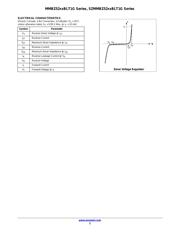
Device Package Shipping
†
ORDERING INFORMATION
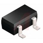
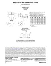
SOT−23
CASE 318
STYLE 8
3
Cathode
1
Anode
MARKING DIAGRAM
See specific marking information in the device marking
column of the Electrical Characteristics table on page 3 o
f
this data sheet.
DEVICE MARKING INFORMATION
M
MMBZ52xxBLT1G SOT−23
(Pb−Free)
3,000 /
Tape & Reel
†For information on tape and reel specifications,
including part orientation and tape sizes, please
refer to our Tape and Reel Packaging Specification
s
Brochure, BRD8011/D.
MMBZ52xxBLT3G SOT−23
(Pb−Free)
10,000 /
Tape & Reel
xxx G
G
xxx = Specific Device Code
M = Date Code
G = Pb−Free Package
SZMMBZ52xxBLT1G SOT−23
(Pb−Free)
3,000 /
Tape & Reel
SZMMBZ52xxBLT3G SOT−23
(Pb−Free)
10,000 /
Tape & Reel
(Note: Microdot may be in either location)
www.onsemi.com
页面指南