
下载
Semiconductor Components Industries, LLC, 2011
November, 2011 − Rev. 8
1 Publication Order Number:
MMBD352LT1/D
MMBD352LT1G,
MMBD353LT1G,
NSVMMBD353LT1G,
MMBD354LT1G,
NSVMMBD354LT1G,
MMBD355LT1G
Dual Hot Carrier Mixer
Diodes
These devices are designed primarily for UHF mixer applications
but are suitable also for use in detector and ultra−fast switching
circuits.
Features
Very Low Capacitance − Less Than 1.0 pF @ Zero V
Low Forward Voltage − 0.5 V (Typ) @ I
F
= 10 mA
AEC Qualified and PPAP Capable
NSV Prefix for Automotive and Other Applications Requiring
Unique Site and Control Change Requirements
These Devices are Pb−Free, Halogen Free/BFR Free and are RoHS
Compliant*
MAXIMUM RATINGS (EACH DIODE)
Rating
Symbol Value Unit
Continuous Reverse Voltage V
R
7.0 V
CC
Maximum ratings are those values beyond which device damage can occur.
Maximum ratings applied to the device are individual stress limit values (not
normal operating conditions) and are not valid simultaneously. If these limits are
exceeded, device functional operation is not implied, damage may occur and
reliability may be affected.
THERMAL CHARACTERISTICS
Characteristic Symbol Max Unit
Total Device Dissipation FR−5 Board,
(Note 1)
T
A
= 25C
Derate above 25C
P
D
225
1.8
mW
mW/C
Thermal Resistance, Junction−to−Ambient
R
q
JA
556 C/W
Total Device Dissipation Alumina
Substrate, (Note 2)
T
A
= 25C
Derate above 25C
P
D
300
2.4
mW
mW/C
Thermal Resistance, Junction−to−Ambient
R
q
JA
417 C/W
Junction and Storage Temperature T
J
, T
stg
−55 to +150 C
1. FR−5 = 1.0 x 0.75 x 0.062 in.
2. Alumina = 0.4 x 0.3 x 0.024 in. 99.5% alumina.
*For additional information on our Pb−Free strategy and soldering details, please
download the ON Semiconductor Soldering and Mounting Techniques
Reference Manual, SOLDERRM/D.
http://onsemi.com
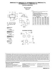
SOT−23 (TO−236)
CASE 318
*Date Code orientation and/or overbar may
vary depending upon manufacturing location.
1
Mxx M G
G
Mxx = Device Code
M = Date Code*
G = Pb−Free Package
(Note: Microdot may be in either location)
MARKING DIAGRAM
See detailed ordering, marking, and shipping information in the
package dimensions section on page 2 of this data sheet.
ORDERING INFORMATION
MMBD352LT1G
STYLE 11
1
ANODE
3
CATHODE/ANODE
2
CATHODE
MMBD353LT1G
NSVMMBD353LT1G
STYLE 19
1
CATHODE
3
CATHODE/ANODE
2
ANODE
MMBD354LT1G
NSVMMBD354LT1G
STYLE 9
3
CATHODE
1 ANODE
ANODE 3
1 CATHODE
2 CATHODE
MMBD355LT1G
STYLE 12
2 ANODE