
下载
© Semiconductor Components Industries, LLC, 2013
December, 2013 − Rev. 13
1 Publication Order Number:
MJE340/D
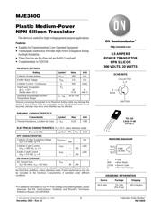
MJE340G
Plastic Medium-Power
NPN Silicon Transistor
This device is useful for high−voltage general purpose applications.
Features
• Suitable for Transformerless, Line−Operated Equipment
• Thermopad Construction Provides High Power Dissipation Rating
for High Reliability
• These Devices are Pb−Free and are RoHS Compliant*
• Complementary to MJE350
MAXIMUM RATINGS
Rating Symbol Value Unit
Collector−Emitter Voltage V
CEO
300 Vdc
Emitter−Base Voltage V
EB
3.0 Vdc
Collector Current − Continuous I
C
500 mAdc
Total Power Dissipation
@ T
C
= 25_C
Derate above 25_C
P
D
20
0.16
W
mW/_C
Operating and Storage Junction
Temperature Range
T
J
, T
stg
–65 to +150
_C
Stresses exceeding those listed in the Maximum Ratings table may damage the
device. If any of these limits are exceeded, device functionality should not be
assumed, damage may occur and reliability may be affected.
THERMAL CHARACTERISTICS
Characteristic Symbol Max Unit
Thermal Resistance, Junction−to−Case
q
JC
6.25
_C/W
ELECTRICAL CHARACTERISTICS (T
C
= 25°C unless otherwise noted)
Characteristic
Symbol Min Max Unit
OFF CHARACTERISTICS
Collector−Emitter Sustaining Voltage
(I
C
= 1.0 mAdc, I
B
= 0)
V
CEO(sus)
300 −
Vdc
Collector Cutoff Current
(V
CB
= 300 Vdc, I
E
= 0)
I
CBO
− 100
mAdc
Emitter Cutoff Current
(V
EB
= 3.0 Vdc, I
C
= 0)
I
EBO
− 100
mAdc
ON CHARACTERISTICS
DC Current Gain
(I
C
= 50 mAdc, V
CE
= 10 Vdc)
h
FE
30 240
−
Product parametric performance is indicated in the Electrical Characteristics for
the listed test conditions, unless otherwise noted. Product performance may not
be indicated by the Electrical Characteristics if operated under different
conditions.
*For additional information on our Pb−Free strategy and soldering details, please
download the ON Semiconductor Soldering and Mounting Techniques
Reference Manual, SOLDERRM/D.
Device Package Shipping
ORDERING INFORMATION
0.5 AMPERE
POWER TRANSISTOR
NPN SILICON
300 VOLTS, 20 WATTS
http://onsemi.com
MJE340G
TO−225
(Pb−Free)
500 Units/Box
MARKING DIAGRAM
Y = Year
WW = Work Week
JE340 = Device Code
G = Pb−Free Package
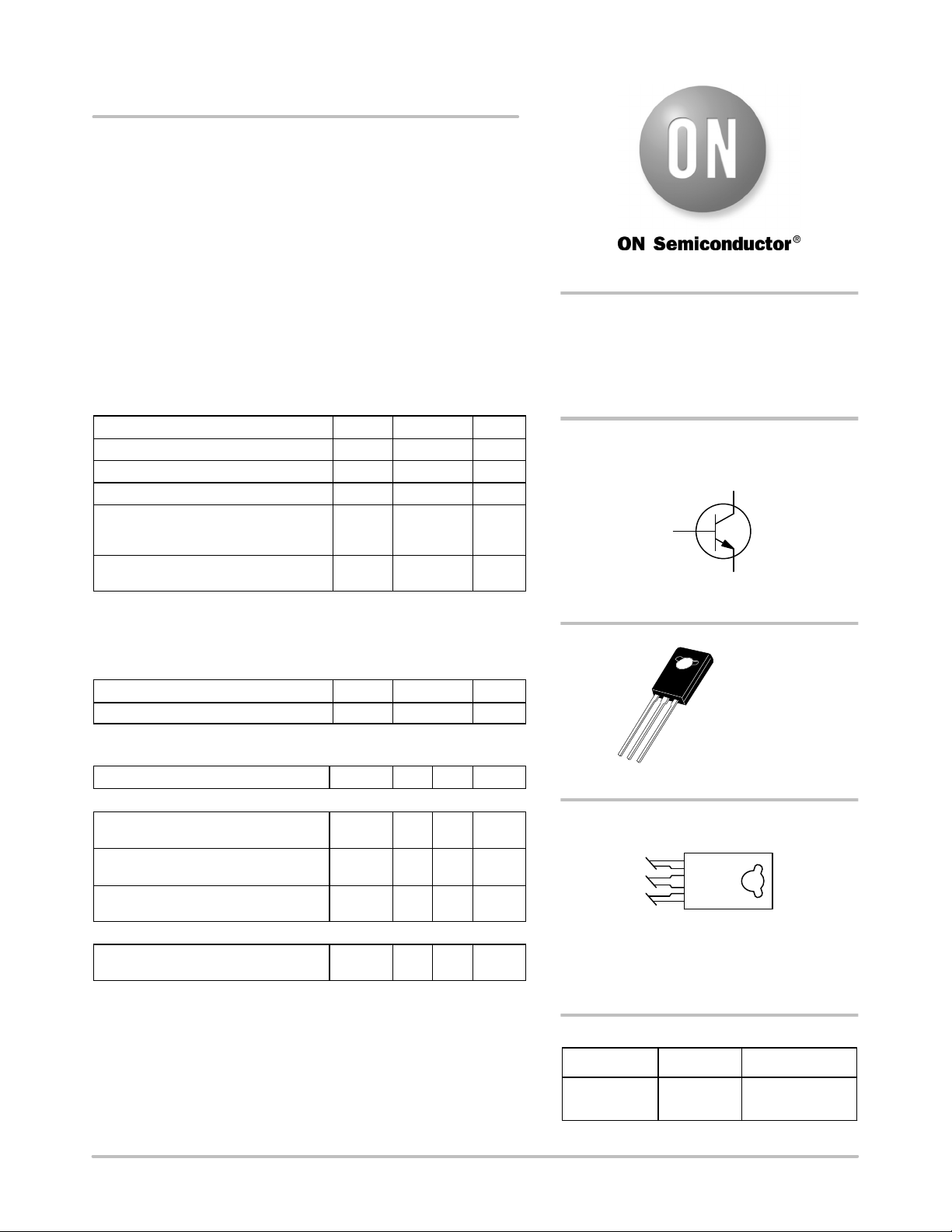
3
BASE
1
EMITTER
COLLECTOR
2, 4
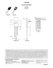
SCHEMATIC
TO−225
CASE 77−09
STYLE 1
1
2
3
YWW
JE340G