
šłčŤĹĹ
 2003 Microchip Technology Inc. DS00248A-page 1
M
AN248
INTRODUCTION
The MCP6S21/2/6/8 family of one, two, six or eight
channel Programmable Gain Amplifiers (PGA) commu-
nicate using a standard 3-wire Serial Peripheral Inter-
face (SPI‚ĄĘ) protocol. This application note shows how
to program the six channel MCP6S26 PGA gains,
channels and shutdown registers using the PIC16C505
microcontroller.
The PIC16C505 microcontroller does not have a hard-
ware SPI module, therefore, a firmware SPI (Bit Bang)
method is used to program the PGA. The MCP6S2X
Evaluation Board was used to develop this application
note firmware. For additional information, refer to the
MCP6S2X Evaluation Board User’s Guide (DS51327),
MCP6S21/2/6/8 PGA data sheet (DS21117) and
PIC16C505 data sheet (DS40192).
COMMUNICATION
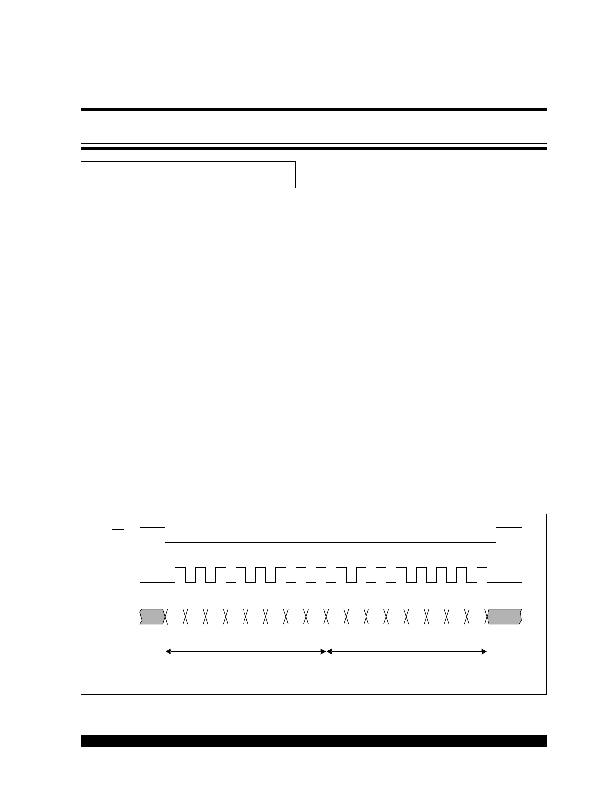
Figure 1 shows the SPI communication format with the
clock idle low and the serial data latched at the rising
edge of the clock. This format is sometimes referred to
as ‚Äú0,0‚ÄĚ mode. Instructions for the MCP6S21/2/6/8
family of PGAs consists of sixteen serial clock cycles
and two serial data bytes. The first byte is the instruc-
tion byte, which consists of register options, such as
Write, Shutdown, Gain and Channel. The second byte
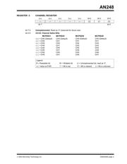
is the data byte, whose three Least Significant Bits
(LSB) are used to program gain or channel. There are
eight gain settings and up to eight channel settings,
depending on the specific device.
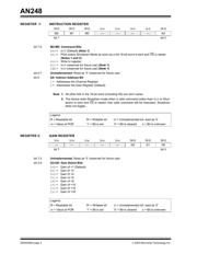
Command bits 7, 6 and 5 of the instruction byte deter-
mines whether to write to the registers or shutdown the
device. A bit configuration of 010 directs the data byte
to be written to the Gain or Channel registers. When
writing to the registers, if command bit 0 is cleared, the
data byte is shifted into the Gain register. If the com-
mand bit 0 is set, the data byte is shifted into the
Channel register.
A 001 command bit configuration shuts down the
device. If shutdown is selected, command bit 0
becomes a ‚Äúdon‚Äôt care‚ÄĚ bit.
Command bits 4, 3, 2 and 1, and data bits 7 through 3,
are not used and are ‚Äúdon‚Äôt cares‚ÄĚ. Refer to Register 1,
Register 2 and Register 3 tables on pages 2 and 3.
FIGURE 1: PGA Instruction byte and data byte programming sequence.
Author: Ezana Haile
Microchip Technology Inc.
12345678910111213141516
bit 7
CS
SCK
SI
Instruction Byte Data Byte
bit 0
bit 7
bit 0
M2
M1 M0
A0
G2
G2
G0
XXXX XXXXX
X = don’t cares
Interfacing MCP6S2X PGAs to PICmicro
¬ģ
Microcontroller