
下载

© 2008 Microchip Technology Inc. DS01177A-page 1
AN1177
INTRODUCTION
Engineers that use op amps in their circuits; especially
those new to analog or op amp circuit design. Also
intended for engineers that want to understand op amp
DC specifications.
Description
This application note covers the essential background
information and design theory needed to design a
precision DC circuit using op amps. Topics include:
• Op Amp DC Specifications
• Circuit Analysis
• Circuit Optimization
• Advanced Topics
• References
This application note is limited to voltage feedback
(traditional) op amps. Those interested in current feed-
back op amps will benefit from the information here; the
DC specifications and op amp DC model have many
similarities.
For those that are interested, a simple circuit for
measuring input offset voltage has been included in
Appendix A: “Input Offset Measurement Circuit”.
DC SPECIFICATIONS
There are a small number of DC specifications that
describe errors at the input of an op amp. This section
organizes these specifications into those related to the
input offset and the others related to input bias
currents.
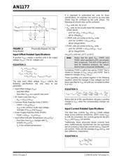
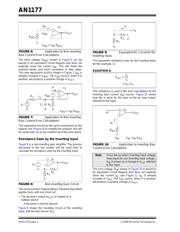
Ideal Op Amp
Figure 1 shows the ideal, DC model for op amps (the
external circuitry is not shown). All error sources are
ignored and the open-loop gain (A
OL
) is infinite. The
output voltage is related to the input voltages as shown
in Equation 1.
FIGURE 1: Ideal, DC Op Amp Model.
EQUATION 1:
When negative feedback is applied, the ideal op amp’s
infinite gain forces V
N
and V
I
to be exactly equal; this is
the virtual short that some authors talk about. [ 1, 2]
When positive feedback is applied (e.g., when used as
a comparator), V
OUT
swings as far negative or positive
as it can (to the rails), depending on the sign of the dif-
ference (V
N
–V
I
).
Op Amp Model with DC Errors
Figure 2 shows a physically based, DC model for op
amps. V
PLUS
and V
MINUS
are the external input volt-
ages, while V
N
and V
I
are the internal input voltages.
V
OST
represents the total input offset voltage error. The
non-inverting bias current (I
BN
) and inverting bias cur-
rent (I
BI
) represent the physical currents seen at each
of the two input pins. A
OL
is the finite DC open-loop
gain.
Author: Kumen Blake
Microchip Technology Inc.
A
OL
V
OUT
V
N
V
I
V
OUT
A
OL
V
N
V
I
–()=
Op Amp Precision Design: DC Errors