
下载

© 2007 Microchip Technology Inc. DS01080A-page 1
AN1080
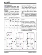
INTRODUCTION
All semiconductor devices have variations over
process. In the case of digital potentiometer devices,
this process variation affects the device resistive
elements (R
AB
-> R
S
and R
W
). These resistive
elements also have variations with respect to voltage
and temperature, which will also be discussed.
This application note will discuss how process, voltage,
and temperature affect the Resistor Network’s
characteristics and specifications. Also, application
techniques will be covered that can assist in optimizing
the operation of the device to improve performance in
the application.
The process technology used also affects the
operational characteristics. We will focus on the
characteristics for devices fabricated in CMOS.
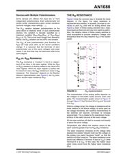
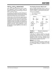
TERMINOLOGY
To assist with the discussions in this application note,
the following terminology will be used. Figure 1
illustrates several of these terms.
Resolution - The number of unique wiper positions
that can be selected between Terminal B and Terminal
A.
Wiper Value - The value in the wiper register which
selects the one wiper switch to close so that the Wiper
Terminal is connected to the Resistor Network.
R
AB
- The total resistance between the A Terminal and
the B Terminal.
R
S
- The Step resistance. This is the change in resis-
tance that occurs between two adjacent wiper register
values. It is also the R
AB
resistance divided by the num-
ber of R
S
resistors (resolution) in the Resistor Ladder.
R
W
- The resistance of the analog switch that connects
the Wiper Terminal to the Resistor Ladder. Each analog
switch will have slightly different resistive characteris-
tics.
Resistor Ladder - Is the serial string of R
S
resistors
between Terminal B and Terminal A. The total resis-
tance of this string equals R
AB
.
Resistor Network - Is the combination of R
S
resistors
and R
W
resistor that create the voltage levels and cur-
rent paths between the A Terminal, B Terminal, and
Wiper Terminal.
R
BW
- The total resistance from Terminal B to the Wiper
Terminal. This resistance equals:
R
S
* (Wiper Register value) + R
W
.
R
AW
- The total resistance from Terminal A to the Wiper
Terminal. This resistance equals:
R
S
* (Full Scale value - Wiper Register value) + R
W
.
Full Scale - When the Wiper is connected to the
closest tap point to Terminal A.
Zero Scale - When the Wiper is connected to the
closest tap point to Terminal B.
FIGURE 1: 8-Bit Resistor Network.
Author: Mark Palmer
Microchip Technology Inc.
W
B
A
n = 0
n = 1
n = 2
n = 254
n = 255
n = 256
(Zero
(Full Scale)
R
S
R
AB
R
BW
R
AW
R
W
R
S
R
S
R
S
R
W
R
W
R
W
R
W
R
W
Scale)
Understanding Digital Potentiometer Resistor Variations