
下载
Semiconductor Components Industries, LLC, 2002
March, 2002 – Rev. 5
1 Publication Order Number:
MC74VHC1GT08/D
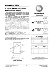
MC74VHC1GT08
2-Input AND Gate/CMOS
Logic Level Shifter
The MC74VHC1GT08 is an advanced high speed CMOS 2–input AND
gate fabricated with silicon gate CMOS technology. It achieves high speed
operation similar to equivalent Bipolar Schottky TTL while maintaining
CMOS low power dissipation.
The internal circuit is composed of three stages, including a buffer
output which provides high noise immunity and stable output.
The device input is compatible with TTL–type input thresholds and the
output has a full 5 V CMOS level output swing. The input protection
circuitry on this device allows overvoltage tolerance on the input, allowing
the device to be used as a logic–level translator from 3.0 V CMOS logic to
5.0 V CMOS Logic or from 1.8 V CMOS logic to 3.0 V CMOS Logic
while operating at the high–voltage power supply.
The MC74VHC1GT08 input structure provides protection when
voltages up to 7 V are applied, regardless of the supply voltage. This
allows the MC74VHC1GT08 to be used to interface 5 V circuits to 3 V
circuits. The output structures also provide protection when V
CC
= 0 V.
These input and output structures help prevent device destruction caused
by supply voltage – input/output voltage mismatch, battery backup, hot
insertion, etc.
• High Speed: t
PD
= 3.5 ns (Typ) at V
CC
= 5 V
• Low Power Dissipation: I
CC
= 1 µA (Max) at T
A
= 25°C
• TTL–Compatible Inputs: V
IL
= 0.8 V; V
IH
= 2.0 V
• CMOS–Compatible Outputs: V
OH
> 0.8 V
CC
; V
OL
< 0.1 V
CC
@Load
• Power Down Protection Provided on Inputs and Outputs
• Balanced Propagation Delays
• Pin and Function Compatible with Other Standard Logic Families
• Chip Complexity: FETs = 64; Equivalent Gates = 15
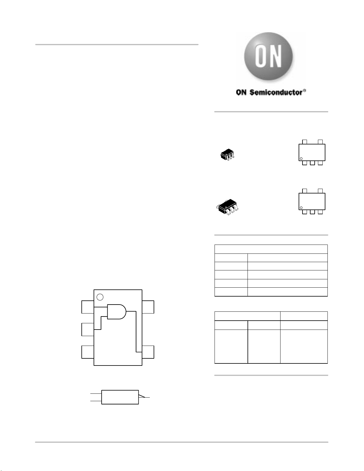
V
CC
IN B
IN A
OUT YGND
IN A
IN B
OUT Y
&
Figure 1. Pinout (Top View)
Figure 2. Logic Symbol
1
2
34
5
PIN ASSIGNMENT
1
2
3 GND
IN B
IN A
4
5V
CC
OUT Y
L
L
H
H
L
H
L
H
FUNCTION TABLE
Inputs Output
AB
L
L
L
H
Y
See detailed ordering and shipping information in the package
dimensions section on page 4 of this data sheet.
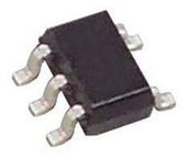
ORDERING INFORMATION
MARKING
DIAGRAMS
SC–88A / SOT–353/SC–70
DF SUFFIX
CASE 419A
Pin 1
d = Date Code
VT
d
TSOP–5/SOT–23/SC–59
DT SUFFIX
CASE 483
Pin 1
d = Date Code
VT
d
http://onsemi.com