
下载

© Semiconductor Components Industries, LLC, 2006
May, 2006 − Rev. 1
1 Publication Order Number:
AND8148/D
AND8148/D
Using the MC74HC589A
as a True SPI−Bus
Peripheral
Prepared by: Fred Zlotnick
ON Semiconductor
INTRODUCTION
When it comes to communicating over a serial bus, there
are three main methods, SPI (Serial Peripheral Interface),
Microwire and I
2
C. The choice is not always easy to make,
and often the designer must use whichever hardware is
available on his micro−controller or peripherals. Art Eck
1
claims that that of the three common interfaces, SPI is
easiest to write code for, and is the fastest protocol.
The SPI−bus was invented in the 1980s as a simple
inexpensive way to communicate with peripherals, with a
minimum of code and absolute simplicity of the receive
function. The SPI−bus is synchronous, with the “master”
device responsible for sending out its own clock signal. The
bus in its most expansive form consists of 4 wires, SCK
(Serial Clock), MISO (Master In Slave Out), MOSI (Master
Out Slave In), and SS (Slave Select). The MC74HC589A is
a MISO (slave) device only. It will not interfere with the SPI
bus use of other master devices in the system, however if
there are no other masters, the system reduces to the MISO
line, the SCK line and n−number of SS lines. The SS lines
can be either a single line controlling a single device or
multiple lines for multiple devices. The Latch Clock pin of
the NLSF589 is the SS pin for SPI operation. In addition, the
MCU needs to provide a logic pin to control the action of the
register, either Parallel Load or Serial Shift, this action is not
an explicit requirement of SPI, however the part will not
function properly, without setting this up. It requires a low
to high transition to move the data that has been stored in the
shift register, into the output latch. Although the device has
an active low Enable pin, it is not necessary to use this pin,
and it may be hard wired low.
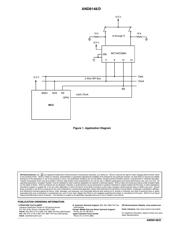
APPLICATION
The diagram below shows the use of an MC74HC589
used to detect key closures in a remote location. We only use
the MISO port of the MCU. The Key closures are applied to
pins A−H. There is no way to determine that a key has either
been opened or closed, so the designer must use a “polling”
technique. The designer initializes the data, then goes out to
the shift register, and reads the data, and looks for a change
from the prior state. The designer must return to the SPI port,
and update the information on a regular basis e.g. every
30ms. The “HC589” has 8 parallel inputs, along with the
various pins for SPI. The diagram shows the switches with
pull up resistors on the parallel port (A−H), so the designer
just needs to supply a logic level to the port. De−bounce is
not explicitly required in hardware. The software engineer
might want to return to the port and poll it again, perhaps
10ms later, to see if the closure records the same data. The
actual software algorithm will be left to the designer. One
further aspect of the design requires the rise and fall times of
the clock signals are observed. At a supply voltage of 5 V, the
rise time must be = 400 ns to assure the clock are recognized
and change state properly. Some designers try to eliminate
rf noise by using RC filtering ion the data and clock lines.
The recommendation is to use a hysteresis gate(s) on the
lines so that the rise and fall time can be met. The circuit is
shown operating at 3.3 V, the only requirement is that both
the MCU and the shift register function at the same voltage,
unless the designer explicitly handles the differences with
logic level translators. The diagram shows the EN (Pin 10)
asserted with a logic level low, and the latch clock (Pin 12)
being asserted with a rising edge applied to this pin. If the
designer is trying to save wires, he can use a single gate
inverter e.g MC74HC1G14 to create a rising edge from the
output enable logic level. Two or more“589s” may be
cascaded to get 16, 24 or more bits of data. If this is done, the
reader should approach this carefully by reading
ON Semiconductor Application Note: AND8144/D and
observing the timing issues.
1. Art Eck, Serial Interface for Embedded Design, Circuit Cellar Online− Jan., 2000
APPLICATION NOTE
http://onsemi.com