
下载
Semiconductor Components Industries, LLC, 2002
January, 2002 – Rev. 3
1 Publication Order Number:
AN531/D
AN531/D
MC1496 Balanced
Modulator
Prepared by: Roy Hejhall
Applications Engineering
INTRODUCTION
The ON Semiconductor MC1496 monolithic balanced
modulator makes an excellent building block for high
frequency communications equipment.
The device functions as a broadband, double–sideband
suppressed carrier balanced modulator without a
requirement for transformers or tuned circuits. In addition to
its basic application as a balanced modulator/demodulator,
the device offers excellent performance as an SSB product
detector, AM modulator/detector, FM detector, mixer,
frequency doubler, phase detector, and more.
The article consists of a general description of the
MC1496, its gain equations, biasing information, and
circuits illustrating typical applications. It is followed by an
appendix containing a detailed mathematical ac and dc
analysis of the device.
Many readers may find that one of the circuits described
in the article will fill the needs of their application. However,
it is impossible to show typical circuits for every possible
requirement, and the detailed analysis given in the appendix
will assist the designer in developing an optimum circuit
for any application within the basic capabilities of the
MC1496.
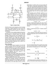
MC1496 General Description
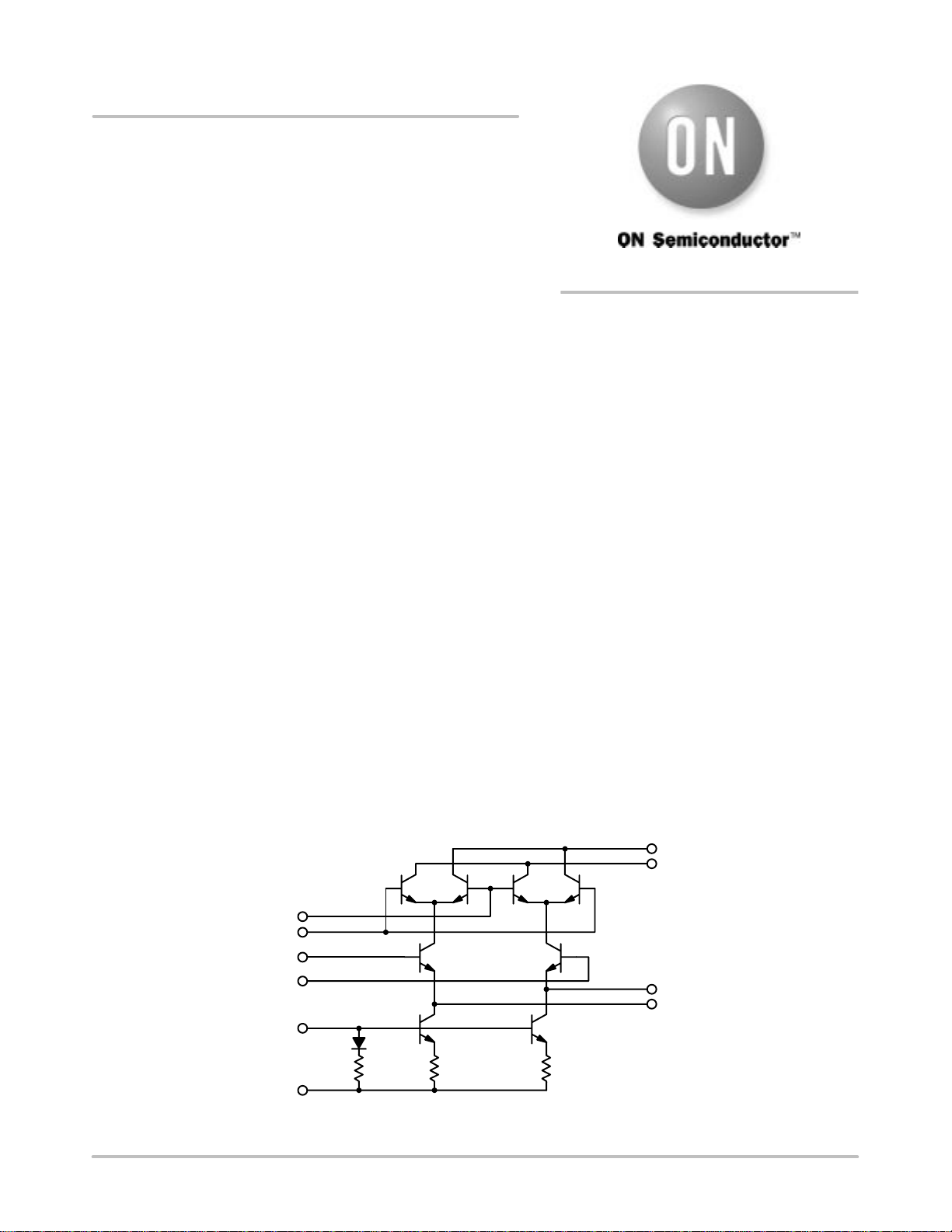
Figure 1 shows a schematic diagram of the MC1496. For
purposes of the analysis, the following conventional
assumptions have been made for simplification: (1) Devices
of similar geometry within a monolithic chip are assumed
identical and matched where necessary, and (2) transistor
base currents are ignored with respect to the magnitude of
collector currents; therefore, collector and emitter currents
are assumed equal.
Referring to Figures 1 and 2, the MC1496 consists of
differential amplifier Q5–Q6 driving a dual differential
amplifier composed of transistors Q1, Q2, Q3 and Q4.
Transistors Q7 and Q8 and associated bias circuitry form
constant current sources for the lower differential amplifier
Q5–Q6.
The analysis of operation of the MC1496 is based on the
ability of the device to deliver an output which is proportional
to the product of the input voltages V
X
and V
Y
. This holds true
when the magnitudes of V
X
and V
Y
are maintained within the
limits of linear operation of the three differential amplifiers in
the device. Expressed mathematically, the output voltage
(actually output current, which is converted to an output
voltage by an external load resistance), V
O
is given by
V
O
KV
X
V
Y
(1)
10(–)
8(+)
4(–)
1(+)
(–)12
(+)6
Q1 Q2 Q3
Q5 Q6
Q7
Q8
Q4
2
3
500500500
Carrier
Input
Signal
Input
V
C
V
S
Bias 5
V
–
14
V
O
, Output
Gain Adjust
Figure 1. MC1496 Schematic
http://onsemi.com
APPLICATION NOTE