
下载
© Semiconductor Components Industries, LLC, 2013
May, 2013 − Rev. 8
1 Publication Order Number:
MC14067B/D
MC14067B
Analog Multiplexers /
Demultiplexers
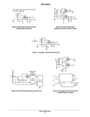
The MC14067 multiplexer/demultiplexer is a digitally controlled
analog switch featuring low ON resistance and very low leakage
current. This device can be used in either digital or analog
applications.
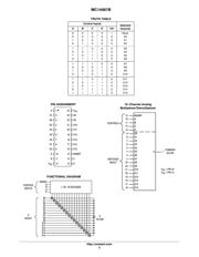
The MC14067 is a 16−channel multiplexer/demultiplexer with an
inhibit and four binary control inputs A, B, C, and D. These control
inputs select 1−of−16 channels by turning ON the appropriate analog
switch (see MC14067 truth table.)
Features
• Low OFF Leakage Current
• Matched Channel Resistance
• Low Quiescent Power Consumption
• Low Crosstalk Between Channels
• Wide Operating Voltage Range: 3 to 18 V
• Low Noise
• Pin for Pin Replacement for CD4067B
• These Devices are Pb−Free and are RoHS Compliant
• NLV Prefix for Automotive and Other Applications Requiring
Unique Site and Control Change Requirements; AEC−Q100
Qualified and PPAP Capable
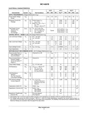
MAXIMUM RATINGS (Voltages Referenced to V
SS
)
Symbol
Parameter Value Unit
V
DD
DC Supply Voltage Range – 0.5 to + 18.0 V
V
in
, V
out
Input or Output Voltage Range
(DC or Transient)
– 0.5 to V
DD
+ 0.5 V
I
in
Input Current (DC or Transient),
per Control Pin
±10 mA
I
sw
Switch Through Current ±25 mA
P
D
Power Dissipation, per Package
(Note 1)
500 mW
T
A
Ambient Temperature Range – 55 to + 125
_C
T
stg
Storage Temperature Range – 65 to + 150
_C
T
L
Lead Temperature
(8–Second Soldering)
260
_C
Stresses exceeding Maximum Ratings may damage the device. Maximum
Ratings are stress ratings only. Functional operation above the Recommended
Operating Conditions is not implied. Extended exposure to stresses above the
Recommended Operating Conditions may affect device reliability.
1. Temperature Derating:
Plastic “P and D/DW” Packages: − 7.0 mW/_C From 65_C To 125_C
This device contains protection circuitry to guard against damage due to high
static voltages or electric fields. However, precautions must be taken to avoid
applications of any voltage higher than maximum rated voltages to this
high−impedance circuit. For proper operation, V
in
and V
out
should be constrained
to the range V
SS
v (V
in
or V
out
) v V
DD
.
Unused inputs must always be tied to an appropriate logic voltage level
(e.g., either V
SS
or V
DD
). Unused outputs must be left open.
http://onsemi.com
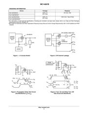
MARKING DIAGRAM
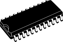
SOIC−24
DW SUFFIX
CASE 751E
A = Assembly Location
WL = Wafer Lot
YY = Year
WW = Work Week
G = Pb−Free Package
See detailed ordering and shipping information in the package
dimensions section on page 5 of this data sheet.
ORDERING INFORMATION
14067B
AWLYYWWG
页面指南