
下载
© Semiconductor Components Industries, LLC, 2014
April, 2014 − Rev. 13
1 Publication Order Number:
MC10EP139/D
MC10EP139, MC100EP139
3.3V / 5V ECL ÷2/4, ÷4/5/6
Clock Generation Chip
Description
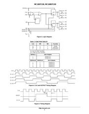
The MC10/100EP139 is a low skew ÷2/4, ÷4/5/6 clock generation chip
designed explicitly for low skew clock generation applications. The
internal dividers are synchronous to each other, therefore, the common
output edges are all precisely aligned.
The common enable (EN
) is synchronous so that the internal dividers
will only be enabled/disabled when the internal clock is already in the
LOW state. This avoids any chance of generating a runt clock pulse on
the internal clock when the device is enabled/disabled as can happen with
an asynchronous control. The internal enable flip−flop is clocked on the
falling edge of the input clock, therefore, all associated specification
limits are referenced to the negative edge of the clock input.
Upon start−up, the internal flip−flops will attain a random state;
therefore the master reset (MR) input may require assertion to ensure
system synchronization. Internal divider design ensures synchronization
between the ÷2/4 and the ÷4/5/6 outputs within a device. All V
CC
and
V
EE
pins must be externally connected to power supply to guarantee
proper operation.
The V
BB
Pin, an internally generated voltage supply, is available to this
device only. For single−ended input conditions, the unused differential
input is connected to V
BB
as a switching reference voltage. V
BB
may also
rebias AC coupled inputs. When used, decouple V
BB
and V
CC
via a
0.01 mF capacitor and limit current sourcing or sinking to 0.5 mA. When
not used, VBB should be left open.
The 100 Series contains temperature compensation.
Features
• Maximum Frequency > 1.0 GHz Typical
• 50 ps Output−to−Output Skew
• PECL Mode Operating Range: V
CC
= 3.0 V to 5.5 V
with V
EE
= 0 V
• NECL Mode Operating Range: V
CC
= 0 V
with V
EE
= −3.0 V to −5.5 V
• Open Input Default State
• Safety Clamp on Inputs
• Synchronous Enable/Disable
• Master Reset for Synchronization of Multiple Chips
• V
BB
Output
• These are Pb−Free Devices
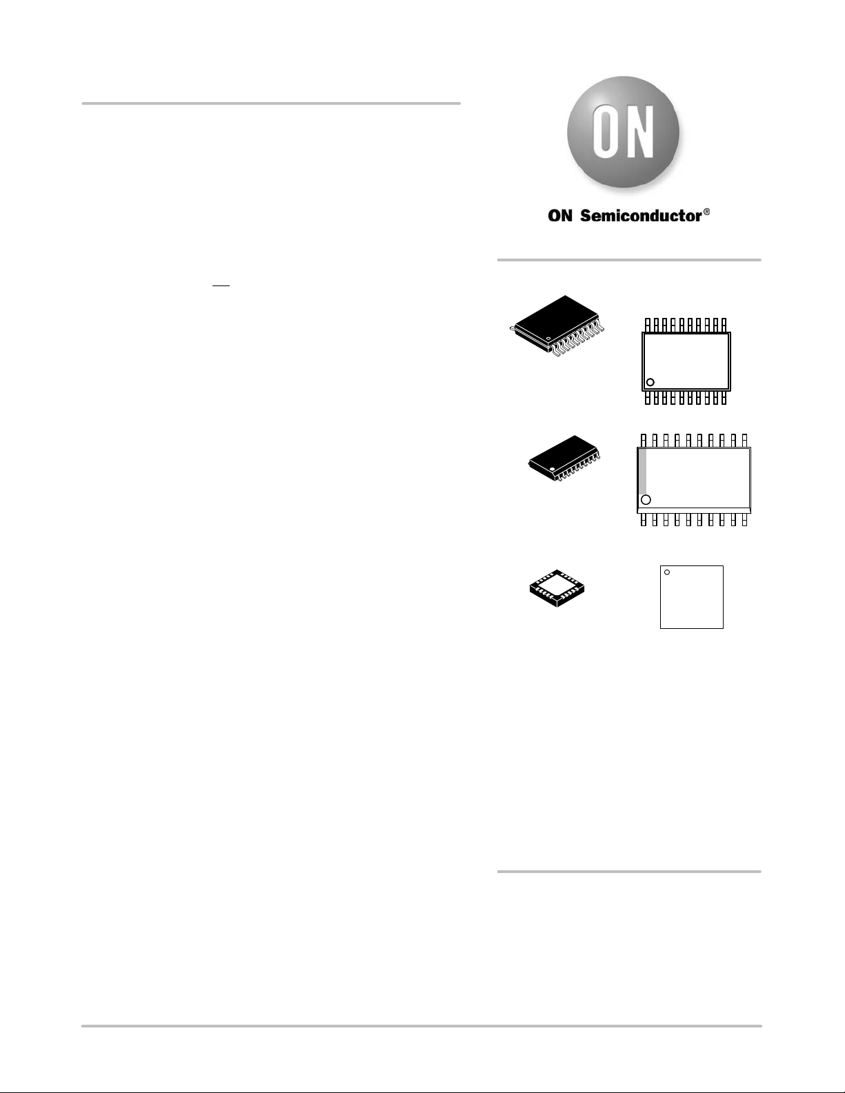
MARKING
DIAGRAMS*
HEP = MC10EP
KEP = MC100EP
XXX = 10 or 100
A = Assembly Location
L,WL = Wafer Lot
Y, YY = Year
W, WW = Work Week
G or G = Pb−Free Package
*For additional marking information, refer to
Application Note AND8002/D.
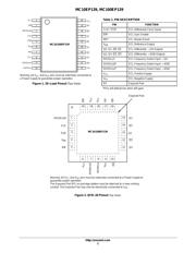
TSSOP−20
DT SUFFIX
CASE 948E
SOIC−20
DW SUFFIX
CASE 751D
1
http://onsemi.com
See detailed ordering and shipping information in the package
dimensions section on page 11 of this data sheet.
ORDERING INFORMATION
20
1
MCXXXEP139
AWLYYWWG
XXXX
EP139
ALYWG
G
1
20
QFN−20
MN SUFFIX
CASE 485E
HEP or KEP
139
ALYWG
G
1
(Note: Microdot may be in either location)
页面指南