


下载

Semiconductor Components Industries, LLC, 2016
January, 2016 − Rev. 1
1 Publication Order Number:
AND8024/D
AND8024/D
Off-Line Critical
Conduction Switching
Power Supply with Voltage
and Current Limiting
Abstract
The need for a small, economical solution for switching
power supplies and for battery chargers has increased. These
applications generally require both voltage limiting and
current limiting. These must be very efficient and produce
a low amount of EMI radiated noise. The MC33364 is
a critical conduction control IC that can be configured in
a resonant turn-off mode to reduce the amount of EMI
generated during turn-off of the power MOSFET.
The MC33341 is a secondary side controller that contains
the band gap reference to provide a very tight tolerance
voltage reference. The MC33341 also allows for current
limiting thus providing an almost square loop of voltage and
current needed for lithium-ion battery charging. Combining
these two devices produces a much more cost-effective
solution than other approaches offer.
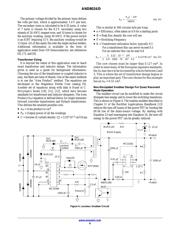
THE CLASSIC APPROACH
In prior years, a very cost efficient and economical design
approach was demanded for battery chargers and power
supplies. The unit had to be current limited on the secondary
side and provide the proper voltage output. The supply often
did not support universal input. One circuit approach to meet
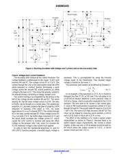
this need is shown in Figure 1. This is a classical blocking
oscillator. This circuit has its roots back to the old vacuum
tube days, and was updated by Bob Haver in 1984 and
presented at various switching power supply seminars [1],
[2]. This is a variable frequency unit that operates in what is
known today as the critical conduction mode.
The unit starts by having the gate of the TMOSt or power
MOSFET turned on by the series resistors R1 and R2. The
current through the primary of the coupled inductor
transformer ramps up linearly. The auxiliary winding on the
transformer is phased to provide positive (in phase) gate
voltage. The TMOS device is “turned off” when the primary
current produces approximately 0.7 V across the source
resistor (Rsource), the bipolar junction transistor (BJT)
becomes forward biased and “turns on”.
When the BJT is “turned on”, the charge on the gate is
removed and the TMOS power FET is “turned off”. The
auxiliary voltage is reversed as the voltage on the primary is
reversed in order to release its stored energy to the
secondary. As long as there is energy flowing to the
secondary, the auxiliary voltage is negative and the gate
voltage is negative. The small signal diode (1N914) in series
with the collector of the BJT keeps the device from operating
in a reverse mode. In lieu of 1N914, a 1N4148 or 1N4150
may be used.
With the TMOS power FET in the “off” mode, the coupled
energy stored in the air gap of the inductor is released to the
secondary. The secondary energy flows to the load by way
of Schottky diode D2. When the coupled energy is depleted,
the voltage across the both the primary, secondary and
auxiliary windings decreases to zero.
The transformer is not a perfect device, so there is a small
amount of energy remaining in the primary. This is the
energy in the leakage inductance of the primary. This causes
the voltage across the transformer to start to ring with the
C
OSS capacitance of the FET. This “turn-off” ring has the
effect of reducing the drain-source voltage of the FET, and
causes the auxiliary winding to develop a positive voltage.
This positive voltage, along with two resistors R1 and R2
places a positive voltage on the gate of the TMOS power
FET; this restarts the energy storage cycle.
www.onsemi.com
APPLICATION NOTE