
下载

Maxim > Design Support > Technical Documents > Application Notes > Prototyping and PC-Board Layout > APP 3940
Keywords: DDR, DDR2, Double Data Rate, SDRAM, SDRAM II, VTT, VDDQ, VTTR, Bus Terminator
APPLICATION NOTE 3940
MAX8632 PCB Layout Optimization
Dec 13, 2006
Abstract: This application note outlines a clear printed-circuit-board (PCB) layout for implementing the
MAX8632 integrated DDR power supply.
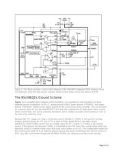
Overview of the MAX8632
The MAX8632 integrates a synchronous-buck controller to generate V
DDQ
main rail, a 3A high-speed
low-dropout (LDO) regulator that can source and sink current to generate VTT bus termination, and a
15mA VTTR reference buffer. The buck controller drives two external n-channel MOSFETs to generate
output voltages down to 0.7V from a 2V to 28V input. The LDO can sink or source up to 1.5A continuous
and 3A peak current. The LDO was designed as a terminator for the DDR memory bus where fast
transients can be expected. This requires a control loop with high bandwidth and a circuit to match.
Page 1 of 13