

下载

Maxim > Design Support > Technical Documents > Application Notes > Basestations/Wireless Infrastructure > APP 4613
Maxim > Design Support > Technical Documents > Application Notes > Communications Circuits > APP 4613
Maxim > Design Support > Technical Documents > Application Notes > High-Speed Interconnect > APP 4613
Keywords: jitter, clock jitter, data jitter, high-speed serial, signal integrity, SERDES, serializer-deserializer, clock
and data recovery, CDR, jitter tolerance, CPRI, common public radio interface, bit error rate, BER, deterministic
jitter, random jitter
APPLICATION NOTE 4613
A Proposed Framework for Measuring, Identifying,
and Eliminating Clock and Data Jitter on High-Speed
Serial Communication Links
By: Hamed Sanogo, Field Applications Engineering Manager
Mar 03, 2010
Abstract: As the new and successful serial-data standards go from fast to very fast, designers must devote a
greater amount of time to the analog aspect of those high-speed signals. It is no longer enough to remain in
the digital domain with ones and zeros. To find and correct conditions that lead to potential problems, and
thereby prevent those problems from showing up in the field, designers must also check the parametric realm
of their designs. Signal integrity (SI) engineers must mitigate or eliminate the effects of timing jitter on system
performance. The following discussion offers a simple and practical procedure for characterizing high-speed
serial data links at 1Gbps and beyond.
A version of this application note appeared on the Electronic Design Magazine website, December 1, 2008.
Introduction
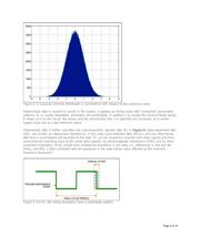
The characterization of a high-speed serial link depends on the ability of the SI engineer to find, understand,
and solve serious jitter problems. In this discussion, we assume that the clock and data recovery (CDR) block
of the PHY (physical layer) or SerDes (serializer-deserializer) device complies with the standards applicable to
that device. In a serial-communication system, the CDR recovers the clock signal from the data stream. Thus,
a key operation is to extract data from the serial data stream and synchronize it with the data-transmitter
clock.
The transmitter always contributes some jitter to the recovered clock, but we assume that contribution to be
minimal. For simplification, therefore, we assume that any jitter seen on the recovered clock was coupled either
onto the link in the cable (as EMI) or within the PCB (as crosstalk).
"Jitter transfer," "jitter tolerance," and "jitter generation" are important measures, but they apply more to PHY
and SerDes devices than to the testing of system channels. We assume that the devices used in our design
meet all device-level compliance testing. We therefore focus on the complete system, as we find a way to
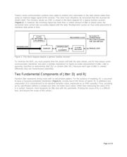
reliably capture serial data at the receiver. We look at system-channel characterization rather than device
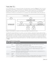
characterization. Such a channel (Figure 1) consists of the transmitter PHY, FR4 (PCB material), connector,
Page 1 of 18