
下载
© Semiconductor Components Industries, LLC, 2012
October, 2012 − Rev. 9
1 Publication Order Number:
MC74LCX16240/D
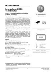
MC74LCX16240
Low-Voltage CMOS
16-Bit Buffer
With 5 V−Tolerant Inputs and Outputs
(3−State, Inverting)
The MC74LCX16240 is a high performance, inverting
16−bit buffer operating from a 2.3 V to 3.6 V supply. The device is
nibble controlled. Each nibble has separate Output Enable inputs
which can be tied together for full 16−bit operation. High impedance
TTL compatible inputs significantly reduce current loading to input
drivers while TTL compatible outputs offer improved switching noise
performance. A V
I
specification of 5.5 V allows MC74LCX16240
inputs to be safely driven from 5.0 V devices. The LCX16240 is
suitable for memory address driving and all TTL level bus oriented
transceiver applications.
Current drive capability is 24 mA at the outputs. The Output Enable
(OEn
) inputs, when HIGH, disable the outputs by placing them in a
HIGH Z condition.
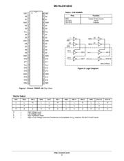
The MC74LCX16240 contains sixteen inverting buffers with
3−state 5.0 V tolerant outputs. The device is nibble controlled with
each nibble functioning identically, but independently. The control
pins may be tied together to obtain full 16−bit operation. The 3−state
outputs are controlled by an Output Enable (OEn
) input for each
nibble. When OEn
is LOW, the outputs are on. When OEn is HIGH,
the outputs are in the high impedance state.
Features
• Designed for 2.3 to 3.6 V V
CC
Operation
• 5.0 V Tolerant − Interface Capability With 5.0 V TTL Logic
• Supports Live Insertion and Withdrawal
• I
OFF
Specification Guarantees High Impedance When V
CC
= 0 V
• LVTTL Compatible
• LVCMOS Compatible
• 24 mA Balanced Output Sink and Source Capability
• Near Zero Static Supply Current in All Three Logic States (10 mA)
Substantially Reduces System Power Requirements
• Latchup Performance Exceeds 500 mA
• ESD Performance: Human Body Model >2000 V;
Machine Model >200 V
• These Devices are Pb−Free, Halogen Free/BFR Free and are RoHS
Compliant
*For additional information on our Pb−Free strategy and soldering details, please
download the ON Semiconductor Soldering and Mounting Techniques
Reference Manual, SOLDERRM/D.
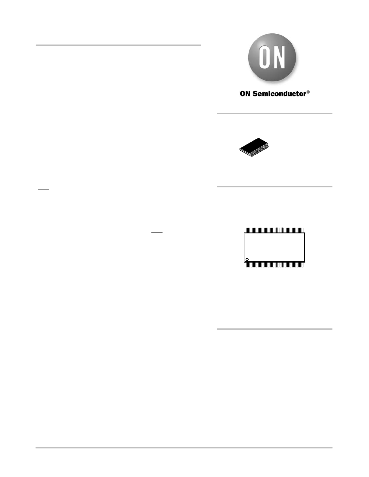
MARKING DIAGRAM
TSSOP−48
DT SUFFIX
CASE 1201
1
48
A = Assembly Location
WL = Wafer Lot
YY = Year
WW = Work Week
G = Pb−Free Package
1
48
LCX16240G
AWLYYWW
See detailed ordering and shipping information in the package
dimensions section on page 3 of this data sheet.
ORDERING INFORMATION
http://onsemi.com
页面指南