


下载

Application Report
SNAA023A–May 2004–Revised April 2013
AN-1275 Optimizing LMX243x Input Sensitivity Using
Simple Matching Techniques
.....................................................................................................................................................
ABSTRACT
The following application report describes how maximum power can be delivered from the voltage
controlled oscillator (VCO) output to the FinRF input of a LMX243x frequency synthesizer by means of
performing a single element match.
Contents
1 Overview ..................................................................................................................... 1
2 Evaluation Methodology .................................................................................................... 3
3 1.0 Optimizing Sensitivity at 5.0 GHz .................................................................................... 3
4 2.0 Optimizing Sensitivity at 6.0 GHz .................................................................................... 4
5 3.0 Optimizing Sensitivity at 2.0 GHz .................................................................................... 6
6 Summary ..................................................................................................................... 7
7 References ................................................................................................................... 8
List of Figures
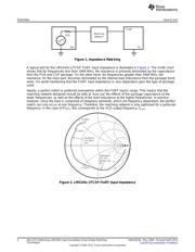
1 Impedance Matching ....................................................................................................... 2
2 LMX243x UTCSP FinRF Input Impedance.............................................................................. 2
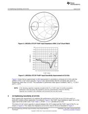
3 1.0 pF Shunt Match at 5.0 GHz........................................................................................... 3
4 LMX243x UTCSP FinRF Input Impedance With 1.0 pF Shunt Match ............................................... 4
5 LMX243x UTCSP FinRF Input Sensitivity Improvement at 5.0 GHz................................................. 4
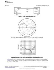
6 0.5 pF Shunt Match at 6.0 GHz........................................................................................... 5
7 LMX243x UTCSP FinRF Input Impedance With 0.5 pF Shunt Match ............................................... 5
8 LMX243x UTCSP FinRF Input Sensitivity Improvement at 6.0 GHz................................................. 5
9 4.7 nH Series Match at 2.0 GHz.......................................................................................... 6
10 LMX243x UTCSP FinRF Input Impedance With 4.7 nH Series Match .............................................. 6
11 LMX243x UTCSP FinRF Input Sensitivity Improvement at 2.0 GHz................................................. 7
List of Tables
1 LMX243x UTCSP FinRF Input Impedance Table V
CC
= EN = 2.50 V, T
A
= +25°C ................................ 7
1 Overview
Maximum power transfer is achieved by designing a matching network that transforms the FinRF input
(load) impedance to an impedance that is equivalent to the VCO output (source) impedance. In most
applications, the VCO has an output impedance equivalent to 50 Ω. Furthermore, the trace impedance of
the printed circuit board (PCB) is typically designed to be 50 Ω. This means that the matching network
should be designed to transform the FinRF input impedance to 50 Ω. Figure 1 demonstrates the principal
of impedance matching (transformation). The VCO output is represented as a Thevenin equivalent of a
voltage source and a 50 Ω series resistance.
All trademarks are the property of their respective owners.
1
SNAA023A–May 2004–Revised April 2013 AN-1275 Optimizing LMX243x Input Sensitivity Using Simple Matching
Techniques
Submit Documentation Feedback
Copyright © 2004–2013, Texas Instruments Incorporated