


下载

Application Report
SNOA497B–September 2007–Revised April 2013
AN-1698 A Specification for EMI Hardened Operational
Amplifiers
.....................................................................................................................................................
ABSTRACT
This application report presents the background, details, and usage of the EMI Rejection Ratio (EMIRR)
parameter.
Contents
1 Introduction .................................................................................................................. 2
2 EMI and Op Amps .......................................................................................................... 2
3 EMIRR Definition ............................................................................................................ 3
4 EMIRR Measurement ...................................................................................................... 4
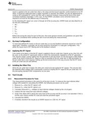
4.1 Op Amp Configuration ............................................................................................. 5
4.2 Applying the RF Signal ............................................................................................ 5
4.3 Isolating the Other Pins ........................................................................................... 5
4.4 Test Circuits ........................................................................................................ 5
5 Measurement Results for the LMV851/LMV852/LMV854 ............................................................. 9
5.1 EMIRR Vs. Frequency ............................................................................................. 9
5.2 EMIRR Vs. Power ................................................................................................ 10
6 Typical Applications and EMIRR ........................................................................................ 11
6.1 Signal Path Application .......................................................................................... 11
6.2 Cell Phone Call ................................................................................................... 12
List of Figures
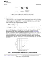
1 Offset Voltage Variation Due to a Detected RF Signal ................................................................ 3
2 Measured Input Referred Offset Voltage Shift vs. Applied RF Peak Level ......................................... 3
3 Coupling the RF Signal to the IN+ Pin Circuit Diagram................................................................ 6
4 Coupling the RF Signal to the IN− Pin Circuit Diagram................................................................ 7
5 Coupling an RF Signal to Either of the Supply Pins Circuit Diagram ................................................ 7
6 Coupling an RF Signal to the Output Pin Circuit Diagram............................................................. 8
7 EMIRR vs. Frequency for IN+, IN−, V
DD
, V
SS
, and OUT................................................................ 9
8 EMIRR vs. RF Input Peak Level for IN+................................................................................ 10
9 Typical Signal Path Application.......................................................................................... 11
10 Pressure Sensor Application............................................................................................. 12
11 Comparing EMI Robustness ............................................................................................. 12
All trademarks are the property of their respective owners.
1
SNOA497B–September 2007–Revised April 2013 AN-1698 A Specification for EMI Hardened Operational Amplifiers
Submit Documentation Feedback
Copyright © 2007–2013, Texas Instruments Incorporated