
下载

1/31
http://onsemi.com
This document is an application note for the LC89091JA which is a digital audio interface receiver.
It describes the following items. Please refer along with the data sheet of the LC89091JA.
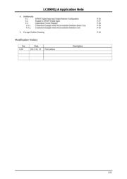
Table of Contents
1. Preparation
1-1. Notes on Implementation P-3
1-2. Oscillation Amplifier Module Connection (XIN, XOUT ) P-3
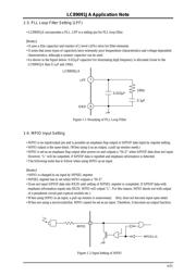
1-3. PLL Loop Filter Setting (LPF) P-4
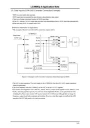
1-4. MPIO Input Setting P-4
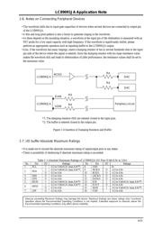
1-5. Data Input to SDIN (A/D Converter Connection Example) P-5
1-6. Notes on Connecting Peripheral Devices P-6
1-7. I/O buffers Absolute Maximum Ratings P-6
1-8. Microcontroller Interface Setting P-7
1-9. Notes on when Microcontroller dosen’t Use P-8
2. System Reset
2-1. Power-on Reset P- 9
2-2. Register Reset (Power-down Mode) P- 9
3. Microcontroller Interface
3-1. Contents of Register P-10
3-2. Write Registers 1 (System) P-11
3-2-1. SYSRST (Reset All Circuits Other than Registers) P-11
3-2-2. PDMODE (Power-down Mode) P-11
3-2-3. AMPOPR (Oscillation Amplifier Operation) P-11
3-2-3-1. Oscillation Amplifier Automatic Stop Function P-12
3-2-4. ADMODE (S/PDIF Receiving Rejection Mode) P-13
3-2-5. ERRWT (ERR Wait Time after PLL Lock) P-13
3-2-6. DATWT (DATAO Wait Time after PLL Unlock) P-15
3-2-7. MPSEL (MPIO Setting) P-16
3-3. Write Registers 2 (Clock) P-17
3-3-1. PLLACC, PLLDIV[1:0], PRSEL[1:0] (PLL and X’tal Clock Setting) P-17
3-3-1-1. Variable Multiple Output P-17
3-3-1-2. Fixed Multiple Output P-18
3-3-1-3. Notes on PLL Clock Setting P-18
3-3-1-4. PLL Clock Switch Timing P-19
3-3-2. XOUTCK (BCKO and LRCKO Output when PLL Unlock) P-20
3-4. Write Register 3 (Data) P-20
3-4-1. DAFORM, DATMUT, NPMODE (DATAO Setting) P-20
3-4-2. DINSEL, THRSEL (S/PDIF Input/Output Data Setting) P-21
3-4-3. GPOSEL[1:0] (GPO Setting) P-21
3-4-4. ERRSEL (ERR Setting) P-22
3-5. Read Register P-25
3-5-1. FSC[3:0] (S/PDIF Input Data Sampling Frequency Calculation Value) P-25
3-5-2. ERRFLG (Error Output Condition) P-25
3-5-3. CS[39:0] (Channel Status Information) P-25
Digital Audio Interface Receiver
Application Note
LC89091JA