

下载
www.latticesemi.com
1
an6065_01.2
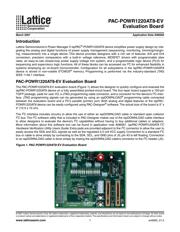
March 2007 Application Note AN6065
PAC-POWR1220AT8-EV
Evaluation Board
© 2007 Lattice Semiconductor Corp. All Lattice trademarks, registered trademarks, patents, and disclaimers are as listed at www.latticesemi.com/legal. All other brand
or product names are trademarks or registered trademarks of their respective holders. The specifications and information herein are subject to change without notice.
Introduction
Lattice Semiconductor’s Power Manager II ispPAC
®
-POWR1220AT8 device simplifies power supply design by inte-
grating the analog and digital functions of power supply management (sequencing, monitoring, trimming/margin-
ing, measurement) into a single device. This device provides designers with a rich set of features: A/D and D/A
conversion, precision comparators with a built-in voltage reference, MOSFET drivers with programmable slew
rates, an easy-to-use closed-loop power supply voltage trim system, and a programmable logic device (PLD) for
sequencing and supervisory logic functions. All of these blocks can be accessed via I
2
C for enhanced flexibility in
systems employing an on-board microcontroller. Configuration for all subsystems in the ispPAC-POWR1220AT8
device is stored in non-volatile E
2
CMOS
®
memory. Programming is performed via the industry-standard JTAG
IEEE 1149.1 interface.
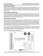
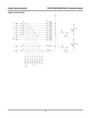
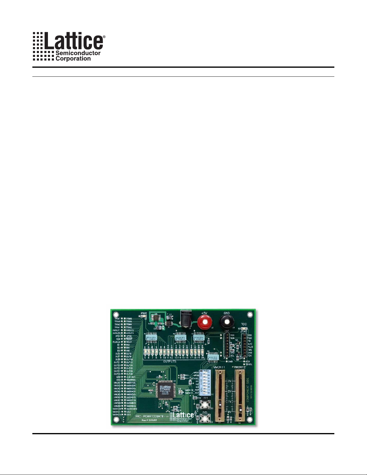
PAC-POWR1220AT8-EV Evaluation Board
The PAC-POWR1220AT8-EV evaluation board (Figure 1) allows the designer to quickly configure and evaluate the
ispPAC-POWR1220AT8 device on a fully assembled printed-circuit board. The four-layer board supports a 100-pin
TQFP package, pads for user I/O, a JTAG programming cable connector, and a connector for the device's I
2
C inter-
face. JTAG programming signals can be generated by using an ispDOWNLOAD
®
programming cable connected
between the evaluation board and a PC’s parallel (printer) port. Both analog and digital features of the ispPAC-
POWR1220AT8 device can be easily configured using PAC-Designer
®
software. The actual size of the board is 5” x
4” (12.5 x 10 cm).
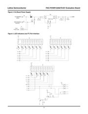
The I
2
C interface includes circuitry to allow the use of either an ispDOWNLOAD cable or standard open collector
I
2
C bus. The I
2
C software utility that is included in PAC-Designer makes use of the ispDOWNLOAD cable interface
to allow designers to evaluate the device’s I
2
C capabilities without having to buy additional cables or adapters.
More information about this software tool can be found in application note AN6067,
ispPAC-POWR1220AT8 I
2
C
Hardware Verification Utility Users Guide.
Extra pads are provided adjacent to the I
2
C connector to allow the user to
easily access the SDA and SCL signals as well as the regulated 3.3 volt VCC supply. Connection to a standard I
2
C
bus or cable is done simply by connecting to the SDA, SCL, and GND pins of J5; pin #3 is left floating. Connection
to an ispDOWNLOAD cable is done simply by mating the ispDOWNLOAD cable’s connector to the I
2
C header (J5).
Figure 1. PAC-POWR1220AT8-EV Evaluation Board