


下载

1 Revision1.0, 2015-07-23
About this document
Scope and purpose
The purpose of this document is to provide a comprehensive functional description and guide to using the
IR1161 single channel synchronous rectification control IC in the output of a switch mode power supply
(SMPS). The scope applies to all technical aspects that should be considered in the design process,
including calculation of external component values, MOSFET selection, PCB layout optimization as well as
additional circuitry that may be added if needed in certain cases.
Intended audience
Power supply design engineers, applications engineers, students.
Table of Contents
1 Introduction and Device Overview ................................................................................................................... 3
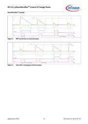
2 ..................................................................................................................................... 4
3 Design and selection of passive components ................................................................................................. 7
3.1 IR1161 VCC supply and current consumption .................................................................................................. 7
3.2 Gate resistor and IC power loss calculation ....................................................................................................... 9
3.3 MOT resistor calculation ......................................................................................................................................... 10
3.4 Thermal Verification ................................................................................................................................................. 10
4 SR MOSFET Power Loss Calculation and Device Selection ......................................................................12
4.1 Body diode conduction loss at turn-on ............................................................................................................. 13
4.2 Channel conduction loss: ........................................................................................................................................ 14
4.3 Body diode conduction loss at turn-off ............................................................................................................. 15
5 Other Application Information.........................................................................................................................18
5.1 Driving a Logic Level MOSFET ............................................................................................................................. 18
5.2 VD filter and delay ..................................................................................................................................................... 19
6 PCB Layout Guidelines and Examples ............................................................................................................22
7 Appendix ................................................................................................................................................................24
IR1161 µ
Design Notes
Authors: Helen Ding
Peter Green
Application Note