
下载

Maxim > Design Support > Technical Documents > Application Notes > T/E Carrier and Packetized > APP 3718
Keywords: T1,E1,template
APPLICATION NOTE 3718
DS26528 and DS26524 Transmit Pulse Control
Dec 22, 2005
Abstract: With the addition of network protection components and/or the need to route signals through
connectors and other PC board requirements, sometimes it is necessary to manipulate the transmit
waveform. The DS26528 and DS26524 contain precise methods for making minor or major changes to
the output pulse. This application note provides the information required to access factory test registers
that allow the transmit waveform to be modified to meet a wide variety of application requirements.
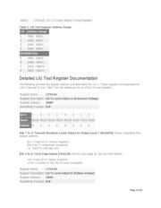
T1 and E1 Transmit Waveform Programmable Sections
The DS26528 and DS26524 contain registers that provide control for the transmit pulse in two major
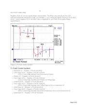
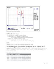
areas: amplitude and timing. T1 and E1 transmit pulses are divided into sections, each of which may be
manipulated to provide the desired waveform. Figure 1 shows how the T1 pulse is divided and the
registers that control each section. Figure 2 provides the same information for the E1 pulse.
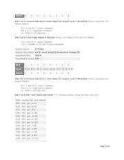
T1 and E1 Transmit Waveform Amplitude Control
The amplitude of the DS26528 and DS26524 transmit pulse may be controlled in two ways:
Adjusting the DAC Gain
The L1TXLAE register bits DAC[3:0] provide positive and negative adjustment of all the T1
or E1 levels simultaneously.
Partial Waveform Level Adjustment
The WLA[3:0] bits of the Level Adjustment registers provide fine tuning of specific sections of
the waveform. The step size of the voltage level will change in proportion to the programmed
DAC gain. If the DAC gain is increased by 10%, then the step sizes will also increase by
10%.
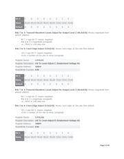
T1 and E1 Transmit Waveform Timing Control
The timing of the DS26528 and DS26524 transmit pulse levels are controlled by the CEA[2:0] bits of the
Level Adjustment registers. Each edge may be moved in both positive and negative directions in
increments of 1/32 of TCLK.
General Recommendations
Modifying the DAC gain is the easiest method of controlling the amplitude of the transmit pulse, because
it will control the entire waveform with only one register change. Using the DAC gain first will allow for
minimal, if any, modifications of the individual Level Adjustment registers.
The maximum output of the DAC will be affected by V
DD
. At lower levels of V
DD
, the maximum DAC
gain setting may be unattainable. Changing V will also affect the maximum voltage attainable by the
Page 1 of 55