
下载

Maxim > Design Support > Technical Documents > Application Notes > Real-Time Clocks > APP 77
Keywords: DS1685,DS1687,DS17285,DS17287,DS17485,DS17487,DS17885,DS17887,extended
ram,user ram, RAM
APPLICATION NOTE 77
DS1685/87 and DS17X85/87 Accessing Extended
User RAM
May 31, 2001
Abstract: This application note describes how to use the extended RAM that is available in some
multiplexed-bus real-time clocks (RTCs).
General Overview
The DS1685/87 and DS17x85/87 include an additional block of extended user RAM. The memory
capacity of each device varies as follows; the DS1685/87 provides 1,024 bits organized in a 128 x 8
block, and the DS17x85/87 provides 16,384, 32,768 or 65,536, bits organized in 2kbits x 8, 4kbits x 8, or
8kbits x 8, blocks respectively.
Register Partitioning
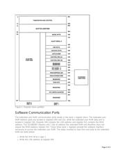
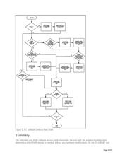
Figure 1 illustrates how the register blocks have been partitioned into two separate banks, bank 0 and
bank 1. A bank select bit, DV0 located in control register 0Ah (bit 4), is used to select which register
bank to make accessible. When DV0 is written to a logic 0, bank 0 is selected and an additional 64
bytes of user RAM can be accessed. However, when DV0 is written to a logic 1, bank 1 is selected and
the additional features, including the extended user RAM, can be accessed. The real time clock (RTC),
control registers, and 50 bytes of user RAM are accessible from either bank, independent of the DV0 bit.
Page 1 of 5