

下载

September 06, 2011 Document No. 001-30920 Rev. *B 1
Innovative Designs Using the RoboClock
®
Family
Application Note Abstract
AN1144 discusses various applications of the Cypress PLL-based, skew-defeating clock buffers known as RoboClock
®
. It is
assumed that the reader has a working understanding of RoboClock.
Overview
Unlike traditional clock buffers, RoboClock enjoys the
advantages of an internal, multi-tapped PLL, which offers
designers two principal advantages: zero propagation delay
and configurable phase control, relative to the reference
clock.
Zero propagation delay is achieved through the presence of
the internal PLL. Because of the properties of PLLs,
RoboClock is able to synchronize itself to an incoming
reference clock, allowing the buffered outputs to be
coincident with the reference input, effectively acting as a
zero propagation delay clock buffer. Conventional clock
buffer solutions, even those that offer low skew, still have a
finite amount of propagation delay. An application example
later in this article demonstrates the constraints these delays
force designers to operate under, and how RoboClock allows
the designer to overcome these constraints.
Configurable phase control of distributed clocks allows the
designer to overcome the debilitating effects of clock skew.
With today’s increasing clock rates, the amount of time
required for a clock signal to travel across a circuit board
becomes a significant portion of the clock period. This clock
skew can result in timing specification violations. RoboClock
offers designers the ability to manipulate the phase of the
distributed clocks, and thereby compensate for clock skew.
Related Documents
For a more complete description of RoboClock as well as its
internal PLL, the reader is encouraged to consult the
following documents for additional information:
CY7B991V Low Voltage Programmable Skew Clock Buffer
datasheet.
CY7B9910/CY7B9920 Low Skew Clock Buffer datasheet.
RoboClock™ and RoboClock II™ Test Mode: Whitepaper
CY7B991/CY7B992 Programmable Skew Clock Buffer
datasheet, published in the Cypress Semiconductor Data
Book.
CY7B9911 High Speed Programmable Skew Clock Buffer
data sheet, published in the Cypress Semiconductor Data
Book.
Using RoboClock to Overcome a
Timing Violation
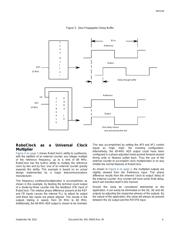
This design example represents how RoboClock can be used
to solve timing margin problems. In this case, the problem is
a register set-up time violation. Represented is an actual
design implemented by a major telecommunications
manufacturer.
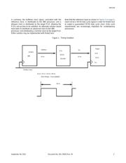
In this application a 33-MHz 486 microprocessor’s address
has a critical path to the registered target PLD through a 6-ns
22V10. As shown in Figure 1 on page 2 the address is
guaranteed valid out of the 486 processor 14 ns after the
initial rising clock edge, after which the address is decoded
by a 22V10 (requiring an additional 6 ns) before needing to
meet a required 10-ns register set-up time of the CPLD.
Examination of the timing constraints shows that no margin is
present-a situation considered unacceptable by the designer.
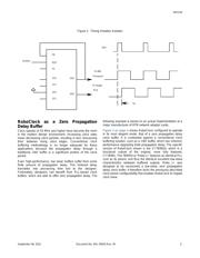
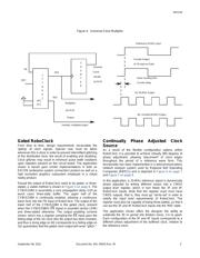
The designer chose the RoboClock implementation shown in
Figure 2 on page 3 in order to solve this timing margin
problem. Essentially, the designer used RoboClock to ‘move
the clock’, adjusting the phase of the 33-MHz clock input to
the target PLD. As is shown, the 1F0 and 1F1 control inputs
are allowed to “float” (the MID logic state), the resultant 1Q0
output is a buffered 33-MHz clock phase-aligned with the
33-MHz reference input. The 2F0 input is tied HIGH and the
2F1 input is allowed to float, configuring the 2Q0 output to be
delayed by one timing unit (t
U
), thus yielding 1.2 ns of margin
to the circuit. The delayed 2Q0 output is then routed to the
clock input of the target PLD, the 1Q0 clock is distributed to
the clock input of the 486 processor.
AN1144
Author: Kelly Mass
Associated Project: No
Associated Application Notes: None